[nextpage title=”Introduction”]
AMD is announcing today its new ATI Radeon HD 2000 Series. This is the first series from AMD/ATI featuring DirectX 10 and five desktop models were announced: Radeon HD 2900 XT for the high-end market (previously known by its codename, R600), Radeon HD 2600 Pro and XT for the mid-range market and Radeon 2400 Pro and XT for the low-end market. While Radeon HD 2900 XT can be found on the market starting today, the other models are just “paper launches”, as they will be released by the end of June, with no specific date set yet. In this article we will explore the details of the new architecture brought by this new series.
It is very important to note that several architecture improvements that are being announced by AMD and by other media refers only to Radeon HD 2900 XT, not being valid for the other two families, HD 2600 and HD 2400.
For a better understanding and comparison with previous technologies, we recommend you to read other two articles, ATI Radeon X1000 Series and GeForce 8 Series Architecture.
Here is a summary on what is new on this family. On the following pages we will talk specifically about the architecture used on each family.
- Shader 4.0 model (DirectX 10). Click here to understand what is new on this new programming model.
- Because it is based on Shader 4.0, it uses a unified shader architecture, where instead of having separated processing units for pixel shader, vertex shader, physics and geometry, it has several “generic” processing units (also called “stream processors”) that can handle any kind of processing. These processors run at the same clock rate as the chip (on GeForce 8 series they run at a different clock rate, higher than the rest of the chip).
- 128-bit HDR (High Dynamic Range). Radeon X1000 series only supported 64-bit HDR. Competing chips from NVIDIA use 128-bit HDR since GeForce 7 series.
- New generation of Avivo – dubbed Avivo HD –, the 2D enhancements from AMD/ATI, featuring HDMI support built-in the graphics chip – i.e., without using an external chip. With an adapter any DVI connector on HD 2000 series-based boards can be transformed into a HDMI connector supporting digital audio output, feature not present on any other video card on the market to date.
- New anti-aliasing mode called Custom Filer Anti-Aliasing or simply CFAA, available up to 24x, competing with Coverage Sample Anti-Aliasing (CSAA) available on GeForce 8 series from NVIDIA.
- Native CrossFire on Radeon HD 2600 and 2900 families.
- 80 nm manufacturing process on Radeon HD 2900 XT and 65 nm manufacturing process on the other models. In fact this is the reason why Radeon HD 2900 XT is being released right now and the other models aren’t.
- New power saving features for the mobile models, called “PowerPlay 7”.
Let’s now talk about the specific architecture and features of each family announced today.
[nextpage title=”Radeon HD 2900 XTX”]
Radeon HD 2900 XT runs at 740 MHz and access its 512 MB GDDR3 memory at 825 MHz (1.65 GHz DDR), using a new 512-bit memory interface, with boosts the memory maximum theoretical transfer rate to 105.6 GB/s – Radeon X1950 XTX has a memory maximum transfer rate of 64 GB/s and GeForce 8800 GTX, of 86.4 GB/s, but the new GeForce 8800 Ultra reaches 103.6 GB/s.
Its unified shader architecture has 320 shader units or “streaming processors” – GeForce 8800 GTX has 128.
In Figure 1 you can have an overall look at the architecture used by Radeon HD 2900 XT.
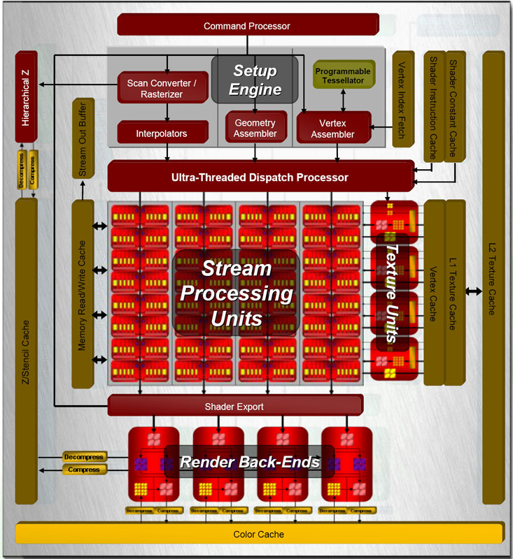 Figure 1: Radeon HD 2900 XT architecture.
In Figure 2 you can have a more in-depth look at how it works. As you can see, it has a dispatch unit that can send up to eight shader instructions to the streaming processors and up to two vertex or texture instructions per clock cycle. And as we will explain below, each one of these shader instructions can actually represent up to six instructions.
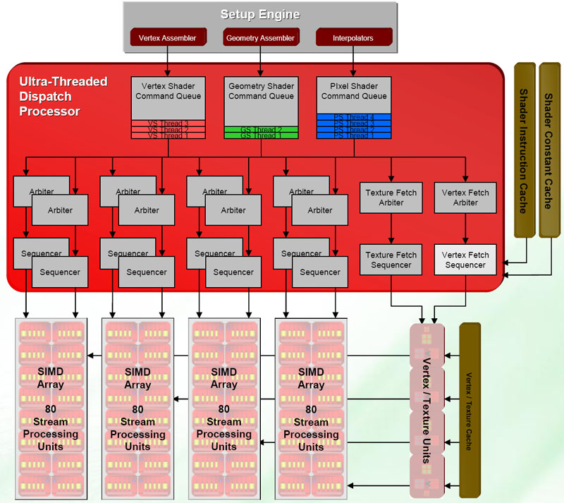 Figure 2: Inside Radeon HD 2900 XT architecture.
The streaming processors are divided into four main groups (called “SIMD arrays”) with 80 processors each, each group connected to two ports of the dispatch unit. These groups are subdivided into 16 units, each unit containing five streaming processors and one branch processing unit. The architecture of each one of these units can be seen in Figure 3.
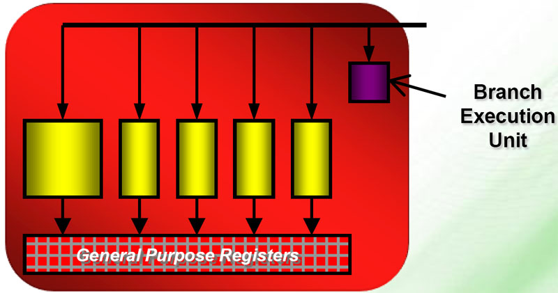 Figure 3: Architecture of each streaming processor unit, containing five processors each.
These units are superscalar, meaning that each streaming processor can be processing several instructions in parallel at the same time. All five processors deal with multiply-add instructions, which are the most common instruction type, while only one (the first one in Figure 3) can also deal with transcendental instructions as well, i.e., log and trigonometric instructions like SIN, COS, LOG, EXP, etc. It is very interesting to note that each streaming processor is, in fact, a small 32-bit floating-point unit.
Another very interesting thing is that each instruction sent to each unit packs six instructions (five math instructions plus one flow control instruction) into a single instruction. So instead of having to send up to six separated instructions to each unit, the dispatch unit can fill all six execution units with just one big instruction. This concept is called VLIW (Very Long Instruction Word).
[nextpage title=”Radeon HD 2900 XTX (Cont’d)”]
In Figure 4 you can have a look at the architecture of Radeon HD 2900 XT texture unit, which supports textures up to 8192 x 8192. This chip features four texture units, each one with eight texture address processors (32 total), 20 texture samplers (80 total) and four texture filter units (16 total). There is also a vertex cache, a L1 texture cache and a 256 KB L2 texture cache.
 Figure 4: Texture unit.
In Figure 5, you can see the details of the rendering unit, which can process up to 32 pixels per clock on the depth/stencil test. Radeon HD 2900 XT has four of these units.
 Figure 5: Rendering unit.
It continues using the memory ring configuration that was introduced on the X1000 series, but now using a fully distributed design instead of a “crossbar switch”. It uses a 1024-bit memory ring, using two separated 512-bit busses, one for reads and another for writes. Another difference is that now PCI Express bus is a client of the memory ring. As already mentioned, Radeon HD 2900 XT uses a 512-bit memory interface, which is achieved by using eight 64-bit memory channels – each channel is connected to a different memory chip.
 Figure 6: Memory interface.
In Figure 7, you can see ATI Radeon HD 2900 XT. One important thing about its installation is that it uses two auxiliary PCI Express power connectors: one regular 6-pin auxiliary PCI Express power connector and a new 8-pin auxiliary PCI Express defined by the new PCI Express 2.0 standard. You have to pay close attention because this new connector resembles the EPS12V power connector available on several power supplies, but the polarity is reversed, i.e., where in the EPS12V connector is ground on the new 8-pin auxiliary PCI Express power connector is +12 V and vice-versa. If you force an EPS12V connector into the 8-pin power connector found on this video card you may burn it (we hope the power supply short-circuit protection can save your day if this happens).
 Figure 7: ATI Radeon HD 2900 XT.
Because it is still manufactured using the 80 nm process it has a typical power consumption of 215 W. AMD recommends at least a 500 W power supply for this baby (750 W if in CrossFire configuration) – however AMD certified some 400 W units to be used with this new video card. A list of certified power supplies can be found here.
Pricing is not bad at all: Radeon HD 2900 XT will reach the market with a suggested price of USD 399.
Below you can find a summary on Radeon HD 2900 XT.
| Model | Clock | Memory Clock | Memory Interface | Memory Configuration | Memory Transfer Rate | Streaming Processors | Suggested Price |
| Radeon HD 2900 XT | 740 MHz | 1.65 GHz (825 MHz x 2) | 512-bit | 512 MB GDDR3 | 105.6 GB/s | 320 | USD 399 |
[nextpage title=”Radeon HD 2600″]
Radeon HD 2600 is the mid-range family of Radeon HD 2000 series and has two models, Pro and XT, with the only difference between the two being the clock rates used. It will reach the market only in late June. This huge delay is due to the new chip manufacturing process (65 nm).
In Figure 8, you can see the architecture used on Radeon HD 2600.
 Figure 8: Radeon HD 2600 architecture.
Radeon HD 2600 main features are:
- 120 streaming processors divided into three SIMD arrays with eight units per array and five processors per unit.
- Six dispatch ports
- Two texture units (16 texture address processors, 40 texture samples and eight texture filter units)
- L2 texture cache of 128 KB
- One rendering unit
- 128-bit memory interface
- Manufactured in 65 nm process
On Figures 9 and 10 you can see Radeon HD 2600 Pro and XT.
 Figure 9: Radeon HD 2600 Pro.
 Figure 10: Radeon HD 2600 XT.
According to AMD Radeon HD 2600 will have a typical power consumption of 45 W (they didn’t say which model they were talking about, Pro or XT).
AMD released two Radeon HD 2600 XT versions, one with 256 MB GDDR4 running at 2.2 GHz (1.1 GHz x 2) and another one with 256 MB GDDR3 running at 1.6 GHz (800 MHz x 2). At the time of its launch, Radeon HD 2600 XT with GDDR4 memory competes directly with GeForce 8600 GT, leaving Radeon HD 2600 XT with GDDR3 with no direct competitor. Radeon HD 2600 Pro competes directly with GeForce 8500 GT.
| Model | Clock | Memory Clock | Memory Interface | Memory Configuration | Memory Transfer Rate | Streaming Processors | Suggested Price |
| Radeon HD 2600 Pro | 600 MHz | 800 MHz (400 MHz x 2) | 128-bit | 256 MB DDR2 | 12.8 GB/s | 120 | USD 99 |
| Radeon HD 2600 XT GDDR3 | 800 MHz | 1.6 GHz (800 MHz x 2) | 128-bit | 256 MB GDDR3 | 25.6 GB/s | 120 | USD 120 |
| Radeon HD 2600 XT GDDR4 | 800 MHz | 2.2 GHz (1.1 GHz x 2) | 128-bit | 256 MB GDDR4 | 35.2 GB/s | 120 | USD 149 |
It is very important to notice that manufacturers can use a memory clock different from what is published above on their models. So you must pay close attention on this spec when comparing video cards based on these new chips, as cards from one manufacturer can be faster than cards from another manufacturer due to the difference on the memory clock used.
[nextpage title=”Radeon HD 2400″]
Radeon HD 2400 is the low-end family in the new Radeon HD 2000 series, also with two models, Pro and XT, with the only difference being the clock used. The most serious difference between the new Radeon HD 2400 family and all other low-end ATI video cards released to date is the memory bus interface: this family uses a 64-bit interface instead of a 128-bit one!
Since video cards using a 64-bit memory interface achieve a performance far lower than their 128-bit counterparts, we still need to do some benchmarking with this new series, because despite its name it may be slower than the “old” Radeon X1300 XT and Radeon X1300 Pro cards!
We know that ATI also released video cards with 64-bit memory interface in the past, but for these cards they used the letters “SE”, so you could clearly identify them.
In Figure 11 you can the Radeon HD 2400 architecture.
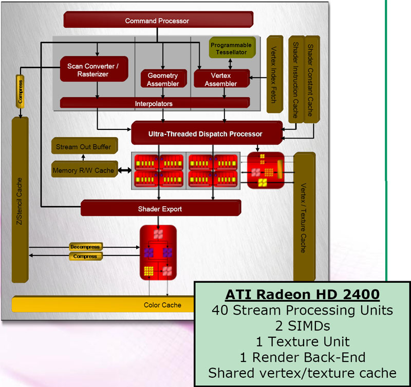 Figure 11: Radeon HD 2400 architecture.
Radeon HD 2400 main features are:
- 40 streaming processors divided into two SIMD arrays with four units per array and five processors per unit.
- Four dispatch ports
- One texture unit (eight texture address processors, 20 texture samples and four texture filter units)
- Unified texture cache
- One rendering unit
- 64-bit memory interface
- Manufactured in 65 nm process
AMD will provide two reference models, one with an active cooler and another with a passive cooler, see Figures 12 and 13. The two boards are identical, the only difference being the cooler.
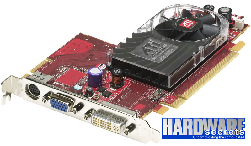 Figure 12: Radeon HD 2400 with active cooling.
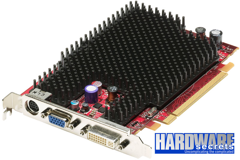 Figure 13: Radeon HD 2400 with passive cooling.
According to AMD Radeon HD 2400 will have a typical power consumption of only 25 W (they didn’t say which model they were talking about, Pro or XT).
Radeon HD 2400 Pro and XT are low-end models, using a 64-bit memory interface. At the moment of its release Radeon HD 2400 XT competes directly with GeForce 7300 GT or with GeForce 8400 GS, while the main competitor for Radeon HD 2400 Pro is GeForce 7300 GS.
| Model | Clock | Memory Clock | Memory Interface | Memory Configuration | Memory Transfer Rate | Streaming Processors | Suggested Price |
| Radeon HD 2400 Pro | 525 MHz | 800 MHz (400 MHz x 2) | 64-bit | 128 MB or 256 MB DDR2 | 6.4 GB/s | 40 | USD 59 |
| Radeon HD 2400 XT | 700 MHz | 1.6 GHz (800 MHz x 2) | 64-bit | 256 MB GDDR3 | 12.8 GB/s | 40 | USD 79 |
It is very important to notice that manufacturers can use a memory clock different from what is published above on their models. So you must pay close attention on this spec when comparing video cards based on this new chip, as cards from one manufacturer can be faster than cards from another manufacturer due to the difference on the memory clock used.
[nextpage title=”Avivo HD”]
Avivo is the name of the 2D enhancements provided by ATI chips on their Radeon X1000 series. These 2D enhancements include things like MPEG2 decoding (for decoding DVDs using the video card instead of the CPU) and de-interlacing (to enhance quality of videos originally aired or created for TV). Click here for full description of the Avivo engine.
Now with the new Radeon HD 2000 series AMD is introducing the second generation of Avivo, called Avivo HD, privileging HD (high definition) contents, making it possible for the graphics chip (GPU) to decode HD-TV, HD-DVD, Blu-Ray and MPEG-4 (a.k.a. H.264) contents (just for the record, HD-DVD and Blu-Ray use a compression algorithm called VC-1).
Why putting DVD, HD-DVD, Blu-Ray and MPEG-4 decoding on the graphics chip is so important? Because it lowers the CPU load, meaning that the computer will work more “light”. It is not only that. When the CPU reaches its maximum load when decoding a disc or video file, it will start dropping frames – i.e., you start getting less than 30 frames per second. What happens is that you see that something is wrong with the video and that the characters movements are somewhat “robotic”.
The problem decoding HD standards is the first decoding stage, entropy decode. On both Avivo and Purevideo HD (the technology equivalent to Avivo on NVIDIA world) this stage is still done by the CPU. With Avivo HD AMD was able to put this stage on the graphics chip as well, as you can see on the comparison chart shown in Figure 14.
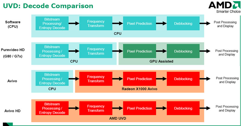 Figure 14: Comparison between Avivo HD and other decoding technologies available.
According to AMD, even new NVIDIA products known today by their codenames G84 and G86 won’t be able do fully decode HD-DVD and Blu-Ray discs, still relying on the system CPU for the first decoding stage, entropy decode. These future chips will be able, however, to fully decode MPEG-4 contents using the graphics chip.
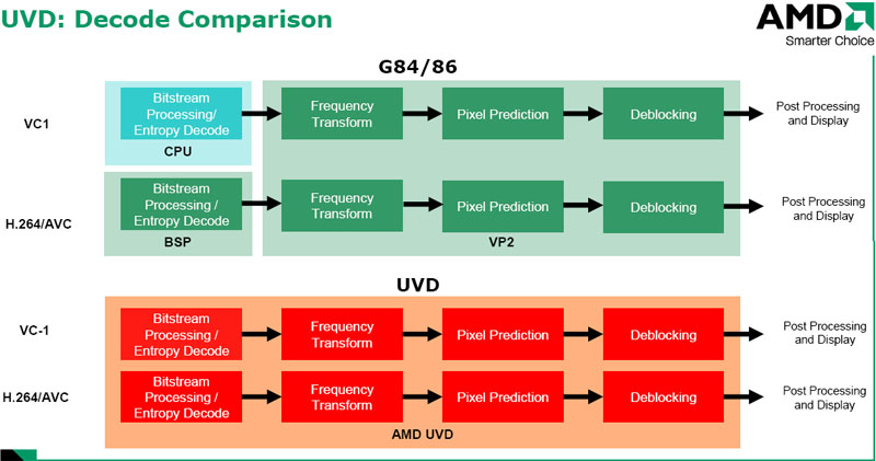 Figure 15: Comparison between Avivo HD and future Purevideo technology that will be used on G86 and G84 products from NVIDIA.
Another advantage pointed out by AMD is that using the GPU for decoding video the system draws less power and with the new Avivo HD you will be able to watch a full-length HD-DVD or Blu-Ray disc on a laptop running on batteries.
A new feature introduced by Avivo HD refers to HDCP, the encryption mechanism to allow playing protected contents such as HD-DVD and Blu-Ray discs. Normally an external ROM chip is needed to store the encryption keys. On the Radeon HD 2000 series these keys are stored inside the chip, lowering the cost of manufacturing video cards compatible with HDCP and improving compatibility with HDCP standard.
At last but not at least, the new Radeon HD 2000 family has HDMI with audio on the same connector without the need of connecting any audio cable to the video card – the video card re-routes digital audio information from the chipset directly to the video card using the PCI Express bus. Other video cards when having a HDMI connector only provide digital video and not audio (there are some video cards with HDMI supporting digital audio, but you need to install an external cable connecting the motherboard SPDIF connector to the video card). Click here to learn more about HDMI.
To use the HDMI connector on any video card from the ATI Radeon HD 2000 series you just need to install an adapter on the DVI connector, like shown in Figure 16.
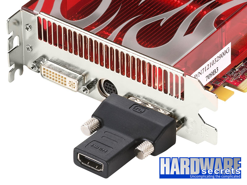 Figure 16: HDMI output on a Radeon HD 2900 XT.
Leave a Reply