[nextpage title=”Introduction”]
SSD (Solid State Drive) units are storage devices that store files and programs just like hard disk drives, but use flash memory chips to store data, instead of storing data on a magnetic disk. Because data is stored electronically rather than magnetically, SSDs are way faster than hard disk drives for two reasons. First, no conversion between magnetic information into electronic information is needed. And second, there are no mechanical parts, so data is readily available, while on hard disk drives you need to wait until the heads move to the area where data is stored, which takes some time. In this short tutorial we will show you how SSD units look like inside and what are their main components.
By the way. Since data is stored inside memory chips, SSD is not a disk, therefore the term “SSD disk” is wrong: prefer the term “SSD unit.”
Let’s first start talking about the external format. SSD’s can be found on several different form factor, i.e., physical sizes. The most common are 2.5” and 1.8,” because these are the same sizes used by hard disk drives targeted to laptops. It is important to know that the first market segment that SSD manufacturers targeted was the mobile market, not the desktop market, for two main reasons: SSD’s consume less power than hard disk drives (this difference may be negligible on a single desktop computer, but for a user running a laptop on batteries, every little difference counts to extend battery life) and are immune to impact (i.e., you can shake, throw and drop SSD’s and your data will still be intact; if you try the same with a hard disk drive you can damage the drive and end up losing all your data).
SSD’s can be also found with several different interfaces, but the SATA interface is the most common.
In Figure 1 we have an example of a 2.5” SSD based on the SATA interface, being the most popular format for SSD units.
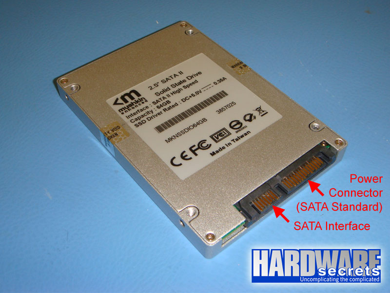
Figure 1: 2.5” SSD.
Now let’s see how the inside of an SSD unit looks like.
[nextpage title=”Inside an SSD Unit”]
In Figure 2, you can see the inside from an SSD unit. There are three main components available: flash memory, controller and buffer. We will give some more details about these components below.
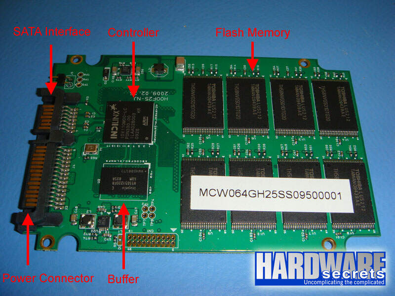
Figure 2: Inside an SSD unit.
Flash Memory
This is where data is stored. Flash memory, which is the kind of memory also found on USB drives (“thumb drives”) and memory cards from digital cameras, don’t lose its contents when power goes off, differently to what occurs with the main RAM from your computer. SSD’s are expensive because lots of this kind of memory is used.
Flash memories can be manufactured under two different technologies, NAND and NOR. The type used on all devices listed above is NAND, and therefore you can see some manufacturers calling flash memory as “NAND.” NOR technology allows running program code and is basically used on cell phones.
Flash memories are available with two different kinds of memory density: SLC (Single-Level Cell) and MLC (Multiple-Level Cell). On SLC chips each storage circuit inside the chip stores only one bit of information, while on MLC chips each circuit stores more than one bit of information. Because of this, MLC chips are cheaper than SLC chips, since one MLC chip can hold more information than one SLC chip. Therefore cheaper SSD units use MLC chips, while more expensive units use SLC devices.
Because data bits inside the chip are closer to each other, MLC chips provide a higher error rate. It is important to note that these errors are not perceived by the user: the controller chip has an error-correction mechanism that detects such errors and automatically fixes them. However, locating and fixing errors takes time, reflecting in a lower performance. In plain English: MLC chips are slower than SLC chips.
Another disadvantage of MLC chips is that they have a shorter life-span compared to SLC chips (flash memories have a finite number of times you can write/erase data to them). Usually SLC chips allow up to 100,000 write/erase cycles before getting unreliable, while MLC chips have a limit of around 10,000 write/erase cycles. Some cheaper chips have lower limits.
Assuming that you have a 64 GB unit, these limits would allow you to write 64 GB 100,000 times on an SLC-based SSD and 64 GB 10,000 times on an MLC-based SSD.
But how long the unit will last? This will depend on the number of write/erase cycles the user performs a day. If we assume that an average user will write 50 GB per day every day, a 64 GB MLC drive would last 35 years (64 GB x 10,000 / 50 GB / 365 days) and a 64 GB SLC drive would last 350 years (64 GB x 100,000 / 50 GB / 365 days). Of course for MLC-based SSD’s with a maximum write/erase cycle lower than 10,000, you will need to adjust the math.
Of course depending on the application you will write way more than 50 GB per day (for example servers), drastically lowering the life-span of the unit. That is why for the enterprise environment (i.e., servers) the kind of SSD that must be used is the SLC. So SLC-based units are classified as “enterprise class”, while MLC-based units are classified as “consumer class”.
Buffer Memory
One chip of low-power SDRAM memory is used to speed up the communications between the controller and the SATA interface.
Controller
This is the heart of the SSD and the component that will tell how fast the unit can be. A few companies manufacture this kind of chip and the most common are Indilinx, Intel, Samsung and JMicron. Controllers organize the flash memory array into “channels,” which in theory can be accessed independently. Thus a controller with 10 channels will probably be faster than a controller that organizes memory into eight channels. We say “probably” because performance depends also on other factors. The controller chip can be also called “SOC” or “System on a Chip.”
Leave a Reply