
Mastering Compact Electronics: A Practical Introduction to HDI PCB Design
The drive toward smaller, smarter devices continues to reshape how engineers approach circuit board layout. From AI-enabled wearables and edge-computing sensors to compact IoT gateways, the need to fit more capability into limited space has become a core requirement in modern hardware development.
High-density interconnect technology meets this need through finer traces, laser-drilled microvias, and sequential build-up processes. Modern HDI PCB design enables boards to support complex circuitry in much smaller footprints than conventional designs. Shorter signal paths, lower power consumption, and higher component density become achievable, which proves especially valuable for high-speed applications in artificial intelligence hardware and real-time processing systems.
What are HDI PCBs
High-density interconnect printed circuit boards, often called HDI PCBs, are a specialized type of circuit board that achieves significantly higher wiring density than standard designs. They accomplish this through smaller trace widths, laser-drilled microvias, and layered construction techniques that allow more connections within a limited area. The result is a board that can handle complex circuitry while remaining much smaller and lighter than traditional alternatives.
This approach supports the ongoing miniaturization of electronics across many industries. Devices that once required larger boards can now incorporate additional features or operate at higher speeds without increasing physical size. HDI PCBs also improve signal performance by shortening interconnect distances, which reduces delays and power loss in high-frequency applications.
Understanding the Main Structural Options
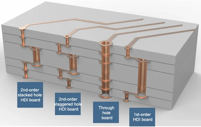
Designers typically classify these boards according to the number of sequential lamination cycles required. The simplest option, often called Type I, connects the outer layer to the first inner layer with microvias while relying on conventional through-holes for the rest of the board. This configuration delivers meaningful density gains with manufacturing processes that remain accessible to most teams.
Moving to two or three build-up cycles adds flexibility. Stacked microvias offer maximum routing density but demand filled and plated structures for mechanical stability, while staggered arrangements are often easier to produce reliably. For most prototyping and small-batch projects, the two-cycle approach strikes an excellent balance between performance and cost.
More advanced constructions with four or more cycles appear in flagship smartphones and enterprise servers, yet they rarely make economic sense for hobbyists or early-stage product development unless ultra-miniaturization is a hard requirement.
Blind and Buried Vias: Unlocking Hidden Routing Space
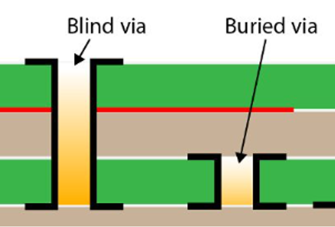
Vias that stop short of passing completely through the board unlock extra routing space. Blind vias connect an outer layer to selected inner layers, while buried vias stay entirely internal. Removing long via stubs reduces signal reflections and frees surface area for component placement.
Production relies on sequential lamination combined with precise laser drilling. Each added layer receives plated and filled microvias before the next cycle. The benefit shows clearly in dense layouts where every square millimeter matters, such as compact AI inference modules or multi-sensor IoT nodes.
Practical Tips to Launch Your First HDI Project
Success begins with thoughtful planning. Define your layer purposes early—separating signals, power, and grounds where possible. Keep traces short and use smooth curves to maintain signal quality. For microvias, respect aspect ratio guidelines to ensure reliable plating.
Here’s a quick starter checklist:
| Parameter | Recommendation |
| Trace/Space | 3–4 mil minimum |
| Microvia Diameter | 0.1–0.15 mm |
| Aspect Ratio | 0.8:1 or better |
| Annular Ring | Minimum 0.1 mm |
| Planes | At least two dedicated reference layers |
Simulation and thorough design rule verification can catch most issues before production.
Common Challenges and How to Overcome Them
New designers often struggle with fine-feature fabrication, heat buildup in crowded layouts, and elevated per-unit costs. Beginning with a modest two-layer build-up on a small project, such as a sensor interface board, allows learning without high risk. Early simulation of signal integrity and thermal behavior identifies problems before boards are ordered.
Cost control comes from limiting build-up cycles and aligning designs with a fabricator’s proven capabilities. Time spent on proper stack-up planning and design-rule checks usually returns value through improved first-pass yields.
Conclusion
High-density interconnect technology empowers engineers and product teams to deliver the compact, high-performance electronics that underpin today’s AI, IoT, and edge-computing innovations. By mastering the fundamentals of microvias, stack-up planning, and signal-integrity best practices, even those new to the discipline can produce reliable boards that meet demanding size and performance targets.