High-Density Electronics: Designing Small Without Sacrificing Performance
Modern electronic systems are increasingly compact while demanding greater functionality. Engineers face the challenge of integrating multiple components into smaller spaces without compromising performance. High-density electronics focus on maximizing capability within limited footprints, allowing devices to be lighter, more portable, and capable of handling complex tasks. This requires careful planning of layouts, power delivery, signal paths, and component selection.
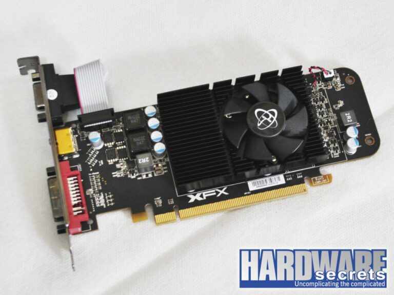
Designing small devices requires careful component selection
Miniature components are central to high-density designs. Microcontrollers, sensors, and memory modules are often used in tightly packed arrangements. Engineers must evaluate each component for size, energy efficiency, and compatibility with the surrounding electronics. Small form factor batteries and power management circuits must also be integrated without creating thermal issues or interference. Component placement is critical to reduce space while maintaining reliable operation; careful attention to spacing, orientation, and interconnection ensures that even highly compact assemblies operate effectively.
Electrical connections are essential for compact systems
As devices shrink, the choice of connectors becomes more important. A circular connector can allow multiple signal and power lines to pass through a single, compact interface. These connectors support high-density layouts by housing many contacts within a small body; they are commonly used in medical devices, industrial equipment, and aerospace electronics where reliability and space efficiency are equally important. Selecting the right connector requires consideration of current rating, environmental exposure, and ease of assembly. Choosing a solution that balances these factors ensures that high-density devices can maintain performance without increasing size or weight.
Board layout and routing play a key role
High-density electronics often rely on multi-layer printed circuit boards. Efficient routing ensures signals reach their destinations without interference, and carefully planned layers can reduce overall device thickness. Placement of components near power and ground planes improves signal stability; spacing and trace width must be calculated to handle the expected current and frequency ranges. Engineers must also consider electromagnetic compatibility to prevent noise from affecting nearby circuits. The layout process requires iterative simulation and testing to optimize both performance and manufacturability.
Thermal management must be integrated into the design
Miniature devices generate heat in smaller volumes, so managing thermal loads is critical. Heat sinks, thermal vias, and conductive substrates help dissipate heat efficiently. Materials with high thermal conductivity can be used for both the board and housing to prevent hotspots. Active cooling may be required in some high-performance applications, but passive strategies are preferred when minimizing size and weight. Careful thermal planning ensures that compact electronics remain reliable throughout their operating life.
Software and firmware support the hardware
The software running on high-density devices must be optimized for limited processing resources and memory. Efficient coding, power management routines, and error-handling algorithms contribute to overall system performance. Integration between hardware and firmware allows the device to operate safely and effectively despite its small form factor. Testing and validation are critical to ensure that the compact design does not create unexpected failures during operation.
High-density electronics combine careful component selection, efficient interconnection, precise board layout, thermal management, and optimized software. Circular connectors provide a practical solution for maintaining reliability and performance in small spaces; they exemplify how a single component can impact overall device design.