How On-Board Audio Works
The South Bridge Chip
Contents
Technically speaking there are two ways of integrating audio on the motherboard. The most common one is using the system CPU to process audio, under a technique called HSP (Host Signal Processing), with the south bridge chip from the chipset providing the necessary interfacing circuit with the external world.
The second way – which nowadays is only seen on few very high-end motherboards – is using a dedicated controller to control and process the audio and thus not using the system CPU for these tasks.
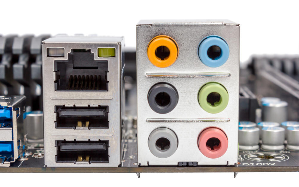
But both the south bridge chip and dedicated controllers aren’t capable of dealing with analog audio, only with digital audio, requiring an external chip – the codec – to perform the interface between the chip and the analog connectors.
The south bridge chip – also called ICH or I/O Controller Hub by Intel –controls the majority of peripheral ports located on the motherboard, like the USB ports and the x1 PCI Express connections. It is a big chip and usually it is located far away from the CPU on the motherboard, normally with a passive heatsink on top. The big chip near the CPU is the north bridge chip.
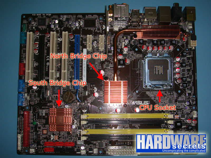
Figure 4: Location of the south bridge chip on a motherboard.
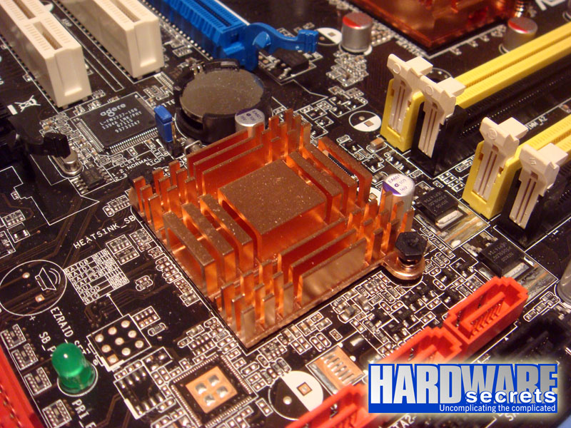
Figure 5: South bridge chip with its passive heatsink.
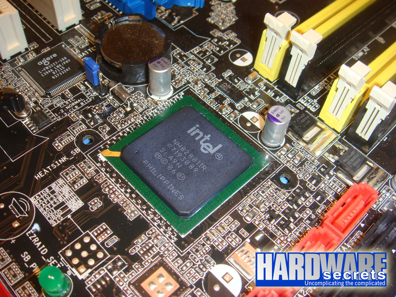
Figure 6: South bridge chip with its passive heatsink removed.
In Figure 7, you can see part of the block diagram of a south bridge chip. Since this block diagram was too big, we are only showing the part that is of interest for our explanations: the audio interface (“Intel High Definition Audio” in Figure 7). This block diagram is from an Intel ICH9 south bridge chip, used by several mainstream chipsets like P965 and P35 (and portrayed on the pictures above).
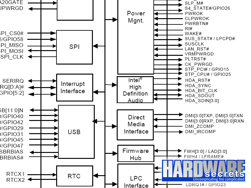
Figure 7: Block diagram of a south bridge chip.
As you can see the audio interface is very simple, providing only a few pins, which are connected to the audio codec located on the motherboard.