
AMD Radeon HD 6950 and 6970 Video Card Review
The AMD Radeon HD 6950 (Cont’d)
Contents
In Figure 5, you can see the video card with its cooler removed and, in Figure 6, a close-up of the voltage regulator circuit. AMD did a great job here, using a high-end configuration, with six phases for the GPU and two phases for the memory chips. The voltage regulator is controlled by a Volterra VT1556MF chip, while each phase is driven by a Volterra VT1636SF chip, which integrated the functions of the traditional three MOSFET transistors that are required (translation: higher efficiency). Unfortunately Volterra doesn’t post datasheets. The voltage regulator also uses ferrite-core coils (which make the regulator to have higher efficiency because they have lower energy loss than iron-core coils) and solid capacitors.
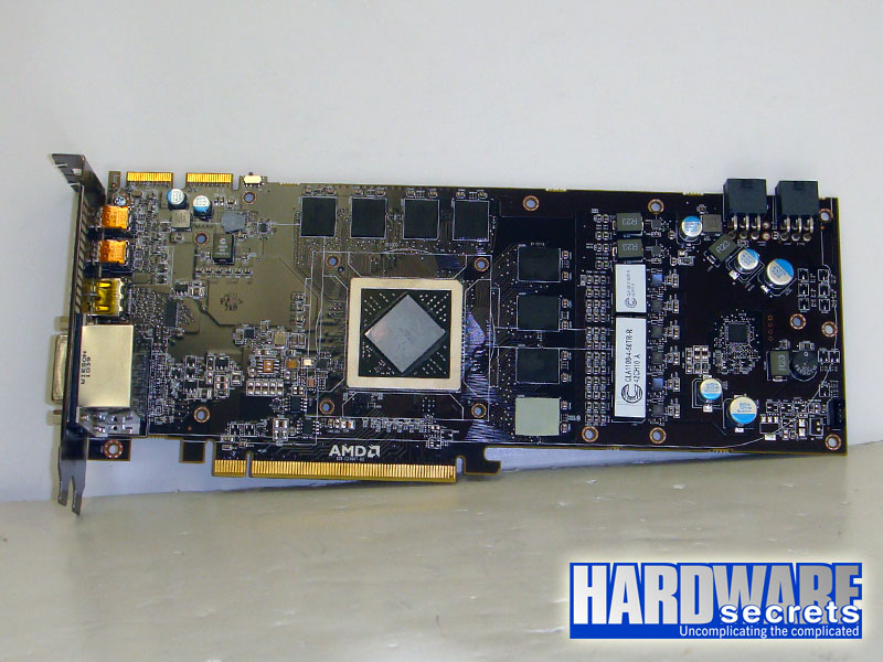 Figure 5: Video card with the cooler removed
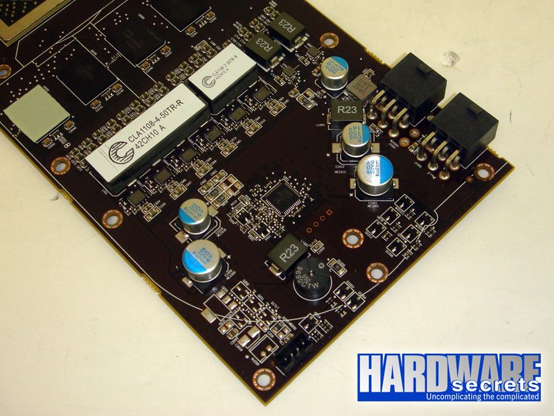 Figure 6: Voltage regulator circuit
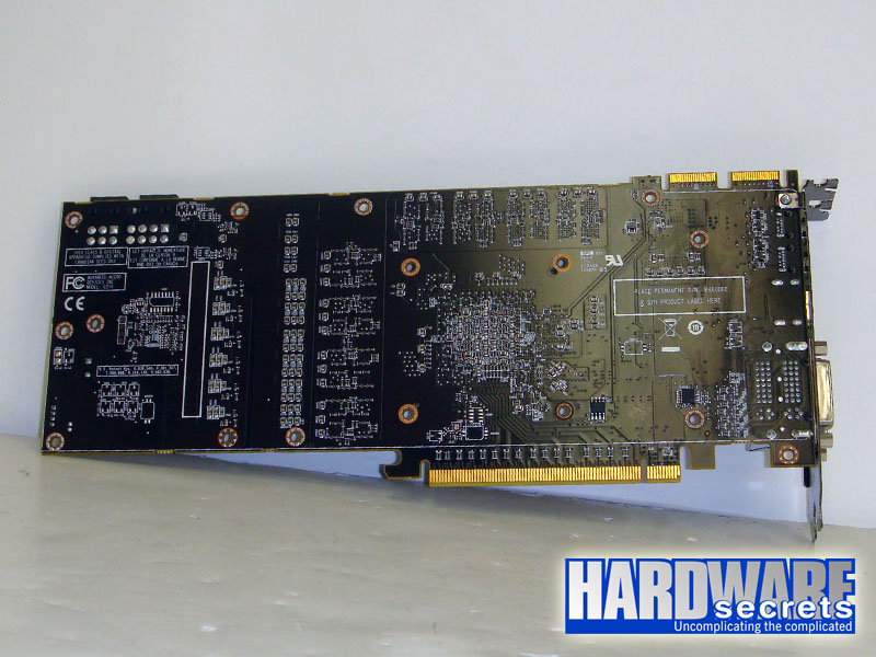 Figure 7: Back of the video card
The GPU cooler can be seen in
Figure 8. It has a copper base using vapor chamber technology, which is the same technology behind heat-pipes, aluminum fins, and a 70 mm radial fan.
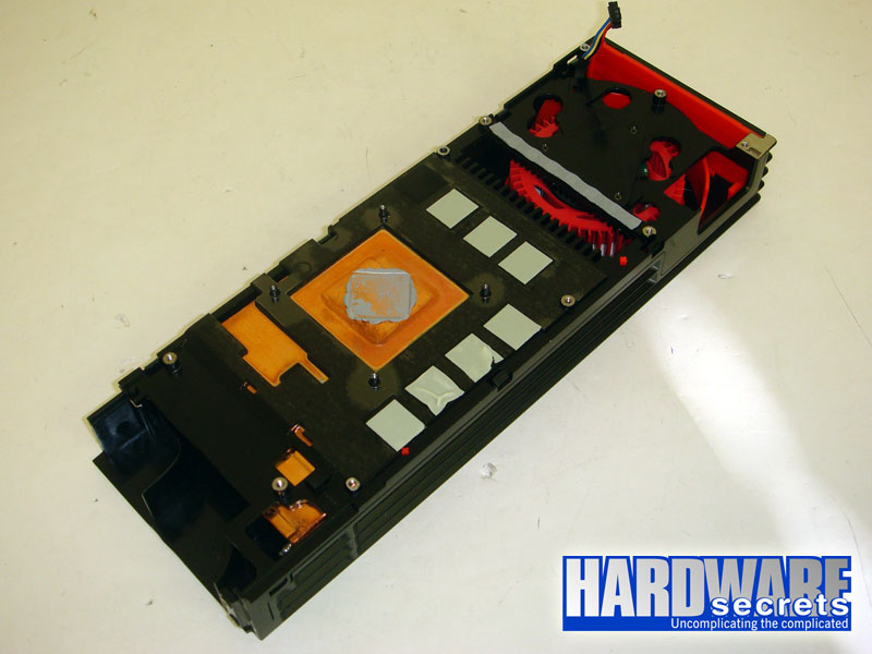 Figure 8: The GPU cooler
The Radeon HD 6850 uses eight 2 Gbit GDDR5 chips, making its 2 GB video memory (2 Gbit x 8 = 2 GB). Each chip is connected to the GPU using a 32-bit data lane, making the video card’s 256-bit memory interface (32 bits x 8 = 256).
The chips used are H5GQ2H24MFR-T2C parts from Hynix, which support up to 2.5 GHz (5 GHz DDR) and since on this video card memory is accessed at 2.5 GHz (5 GHz DDR), there is no margin for you to increase the memory clock rate while keeping the chips inside the maximum they support. Of course you can always try to overclock the memory chips above their specs.
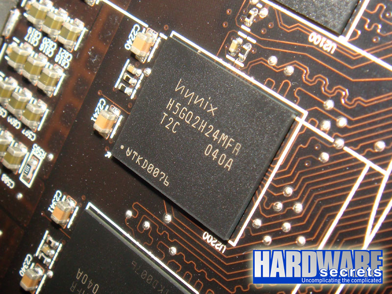 Figure 9: Memory chips
Now let’s take a look at the Radeon HD 6970.