• Skip to primary navigation
  • Skip to main content
  • Skip to primary sidebar
  • Skip to footer
Hardware Secrets

Hardware Secrets

Uncomplicating the complicated

  • Case
  • Cooling
  • Memory
  • Mobile
    • Laptops
    • Smartphones
    • Tablets
  • Motherboard
  • Networking
  • Other
    • Audio
    • Cameras
    • Consumer Electronics
    • Desktops
    • Museum
    • Software
    • Tradeshows & Events
  • Peripherals
    • Headset
    • Keyboard
    • Mouse
    • Printers
  • Power
  • Storage
Home » ADATA BN-550 Power Supply Review

ADATA BN-550 Power Supply Review

[nextpage title=”Introduction”]

ADATA, a traditional memory manufacturer, is entering the power supply market, and its units should arrive in the North American market in the third quarter of this year. They will be selling two series, BN, with models from 400 W to 550 W, and HM, with models from 550 W to 1,200 W. Both series are 80 Plus Bronze-certified, and models from the HM series have a modular cabling system, a feature not available on the BN series. We had the privilege of receiving their BN-550 model before the official release in the United States. Let’s see if this unit is a good product.

The ADATA power supplies are manufactured by HEC/Compucase, and the BN-550 is a rebranded HEC-550TB-2WX unit.

ADATA BN-550 power supplyFigure 1: ADATA BN-550 power supply

ADATA BN-550 power supply
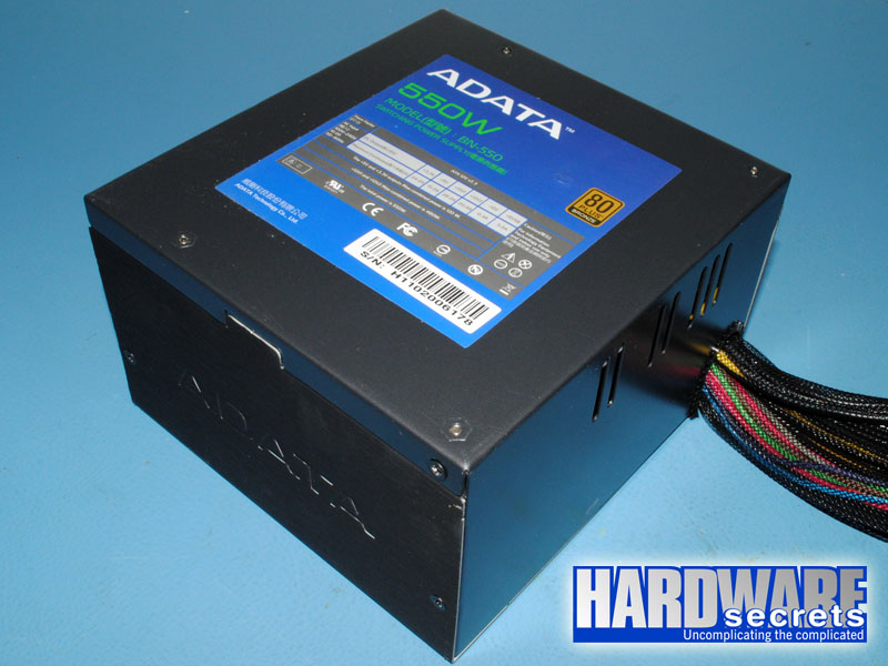
Figure 2: ADATA BN-550 power supply

The ADATA BN-550 is 5.5” (140 mm) deep, using a 120 mm sleeve bearing fan on its bottom (Young Lin Tech DFS122512M, 1,500 rpm, 63.86 cfm, 29.93 dBA).

The cables are permanently attached to the power supply, and they use nylon sleeves. This power supply comes with the following cables:

  • Main motherboard cable with a 20/24-pin connector, 18.1” (46 cm) long
  • One cable with two ATX12V connectors that together form an EPS12V connector, 18.1” (46 cm) long
  • Two cables, each with one six/eight-pin connector for video cards, 18.1” (46 cm) long
  • One cable with four SATA power connectors, 17.7” (45 cm) to the first connector, 5.9” (15 cm) between connectors
  • One cable with three SATA power connectors, 17.7” (45 cm) to the first connector, 5.9” (15 cm) between connectors
  • One cable with two peripheral standard power connectors, 17.7” (45 cm) to the first connector, 5.9” (15 cm) between connectors
  • One cable with two peripheral standard power connectors and one floppy disk drive power connector, 17.7” (45 cm) to the first connector, 5.9” (15 cm) between connectors

All wires are 18 AWG, which is the correct gauge to be used, with the main motherboard connector using thicker wires (16 AWG) for the +3.3 V (orange) output.

The cable configuration is satisfactory for a 550 W product, but we’d like to see more peripheral power connectors.

ADATA BN-550 power supplyFigure 3: Cables

Let’s now take an in-depth look inside this power supply.

[nextpage title=”A Look Inside the ADATA BN-550″]

We decided to disassemble this power supply to see what it looks like inside, how it is designed, and what components are used. Please read our Anatomy of Switching Power Supplies tutorial to understand how a power supply works and to compare this power supply to others.

On this page we will have an overall look, and then in the following pages we will discuss in detail the quality and ratings of the components used.

ADATA BN-550 power supplyFigure 4: Top view

ADATA BN-550 power supplyFigure 5: Front quarter view

ADATA BN-550 power supplyFigure 6: Rear quarter view

ADATA BN-550 power supplyFigure 7: The printed circuit board

[nextpage title=”Transient Filtering Stage”]

As we have mentioned in other articles and reviews, the first place we look when opening a power supply for a hint about its quality, is its filtering stage. The recommended components for this stage are two ferrite coils, two ceramic capacitors (Y capacitors, usually blue), one metalized polyester capacitor (X capacitor), and one MOV (Metal-Oxide Varistor). Very low-end power supplies use fewer components, usually removing the MOV and the first coil.

In this power supply, this stage is flawless. It has two X capacitors, two Y capacitors, and one MOV more than the minimum required.

ADATA BN-550 power supplyFigure 8: Transient filtering stage (part 1)

ADATA BN-550 power supplyFigure 9: Transient filtering stage (part 2)

In the next page we will have a more detailed discussion about the components used in the ADATA BN-550.

[nextpage title=”Primary Analysis”]

On this page we will take an in-depth look at the primary stage of the ADATA BN-550. For a better understanding, please read our Anatomy of Switching Power Supplies tutorial.

This power supply uses one KBU10J rectifying bridge on its primary, which is attached to an individual heatsink. This component supports up to 10 A at 75° C, so in theory, you would be able to pull up to 1,115 W from a 115 V power grid. Assuming 80% efficiency, the bridge would allow this unit to deliver up to 920 W without burning itself out. Of course, we are only talking about this component, and the real limit will depend on all the other components in this power supply.

ADATA BN-550 power supplyFigure 10: Rectifying bridge

The a
ctive PFC circuit uses two IPP60R190C6 MOSFETs, each supporting up to 20.2 A at 25° C or up to 12.8 A at 100° C (note the difference temperature makes) in continuous mode, or up to 59 A in pulse mode at 25° C. These transistors present a 190 mΩ resistance when turned on, a characteristic called RDS(on). The lower this number the better, meaning that the transistor will waste less power, and the power supply will have a higher efficiency.

ADATA BN-550 power supplyFigure 11: Active PFC transistors

The electrolytic capacitor that filters the output of the active PFC circuit is from CapXon and labeled at 85° C.

In the switching section, two FDP18N50 MOSFETs are used in the traditional two-transistor forward configuration, each supporting up to 18 A at 25° C or up to 10.8 A at 100° C (note the difference temperature makes) in continuous mode, or up to 72 A in pulse mode at 25° C, with an RDS(on) of 265 mΩ.

ADATA BN-550 power supplyFigure 12: One of the switching transistors

The primary is controlled by an FAN4800 active PFC/PWM combo controller.

ADATA BN-550 power supplyFigure 13: Active PFC/PWM combo controller

Let’s now take a look at the secondary of this power supply.

[nextpage title=”Secondary Analysis”]

The ADATA BN-550 has five Schottky rectifiers attached to its secondary heatsink.

The maximum theoretical current each line can deliver is given by the formula I / (1 – D) where D is the duty cycle used and I is the maximum current supported by the rectifying diode. As an exercise, we can assume a duty cycle of 30%.

The +12 V output uses two SBR30A50CT Schottky rectifiers (30 A, 15 A per internal diode at 125°, 0.55 V maximum voltage drop), giving us a maximum theoretical current of 43 A or 514 W for this output.

The +5 V output uses one PFR40V60CT Schottky rectifier (40 A, 20 A per internal diode at 120° C, 0.55 V maximum voltage drop), giving us a maximum theoretical current of 29 A or 143 W for this output.

The +3.3 V output uses two STPS30L45CT Schottky rectifiers (30 A, 15 A per internal diode at 135° C, 0.74 V maximum voltage drop), giving us a maximum theoretical current of 43 A or 141 W for this output.

ADATA BN-550 power supplyFigure 14: The +3.3 V, +5 V, and +12 V rectifiers

This power supply uses a PS223 monitoring integrated circuit, which supports over voltage (OVP), under voltage (UVP), over current (OCP), and over temperature (OTP) protections. This chip has four OCP channels, one for +3.3 V, one for +5 V, and two for +12 V, correctly matching the number of +12 V rails advertised by the power supply manufacturer (two).

ADATA BN-550 power supplyFigure 15: Monitoring circuit

The electrolytic capacitors available in the secondary are from Teapo and Su’scon, and labeled at 105° C.

[nextpage title=”Power Distribution”]

In Figure 15, you can see the power supply label containing all the power specs.

ADATA BN-550 power supplyFigure 16: Power supply label

This power supply is sold as having two +12 V rails, which is correct, since this unit has two +12 V over current protection circuits (see previous page). Click here to understand more about this subject.

The two +12 V rails are distributed like this:

  • +12V1 (solid yellow wire): Main motherboard cable, one of the ATX12V connectors, one of the video card power cables, and the SATA and peripheral power connectors
  • +12V2 (yellow/blue wire): The other ATX12V connector and the other video card power cable

This distribution is adequate.

How much power can this unit really deliver? Let’s find out.

[nextpage title=”Load Tests”]

We conducted several tests with this power supply, as described in the article Hardware Secrets Power Supply Test Methodology.

First we tested this power supply with five different load patterns, trying to pull around 20%, 40%, 60%, 80%, and 100% of its labeled maximum capacity (actual percentage used listed under “% Max Load”), watching the behavior of the reviewed unit under each load. In the table below, we list the load patterns we used and the results for each load.

If you add all the powers listed for each test, you may find a different value than what is posted under “Total” below. Since each output can have a slight variation (e.g., the +5 V output working at +5.10 V), the actual total amount of power being delivered is slightly different than the calculated value. In the “Total” row, we are using the real amount of power being delivered, as measured by our load tester.

The +12VA and +12VB inputs listed below are the two +12 V independent inputs from our load tester. During this test, the +12VA input was connected to the power supply +12V1 rail, and the +12VB input was connected to the power supply +12V1 and +12V2 rails (EPS12V connector).

Input Test 1 Test 2 Test 3 Test 4 Test 5
+12VA 4 A (48 W) 8 A (96 W) 12 A (144 W) 16.5 A (198 W) 20.5 A (246 W)
+12VB 4 A (48 W) 8 A (96 W) 12 A (144 W) 16 A (192 W) 20.5 A (246 W)
+5V 1 A (5 W) 2 A (10 W) 4 A (20 W) 5 A (25 W) 6 A (30 W)
+3.3 V 1 A (3.3 W) 2 A (6.6 W) 4 A (13.2 W) 5 A (16.5 W) 6 A (19.8 W)
+5VSB 1 A (5 W) 1 A (5 W) 1.5 A (7.5 W) 2 A (10 W) 2.5 A (12.5 W)
-12 V 0.5 A (6 W) 0.5 A (6 W) 0.5 A (6 W) 0.5 A (6 W) 0.5 A (6 W)
Total 114.8 W 218.5 W 332.6 W 442.2 W 550.8 W
% Max Load 20.9% 39.7% 60.5% 80.4% 100.1%
Room Temp. 45.2° C 44.8° C 44.4° C 45.1° C 48.0° C
 PSU Temp. 46.7° C 44.6° C 44.9° C 46.1° C 49.5° C
Voltage Stability Pass Pass Pass Pass Pass
Ripple and Noise Pass Pass Pass Pass Pass
AC Power 135.5 W 253.7 W 390.2 W 528.2 W 674.0 W
Efficiency 84.7% 86.1% 85.2% 83.7% 81.7%
AC Voltage 116.3 V 115.1 V 113.2 V 111.6 V 110.1 V
Power Factor 0.987 0.958 0.973 0.983 0.989
Final Result Pass Pass Pass Pass Pass

The ADATA BN-550 can really deliver its labeled wattage.

Efficiency was high when we pulled between 20% and 80% of the labeled wattage (i.e., between 110 W and 440 W), ranging from 83.7% and 86.1%. At 550 W, efficiency dropped to 81.7%, which is close enough to the 82% minimum required for the 80 Plus Bronze certification.

Voltage regulation was very good, with all positive voltages within 3% of their nominal values, except for the +5 V output during tests three, four, and five (but it was still inside the proper range; the -12 V output was outside this tighter regulation during tests one and two but was still inside the proper range as well). This means that voltages were closer to their nominal values than required by the ATX12V specification, which says positive voltages must be within 5% of their nominal values and negative voltages must be within 10% of their nominal values.

Noise and ripple levels were always below the maximum allowed, but a little too high at the +12 V outputs for us to consider this unit as “flawless.” Below you can see the results for the power supply outputs during test number five. The maximum allowed is 120 mV for +12 V and -12 V outputs, and 50 mV for +5 V, +3.3 V and +5VSB outputs. All values are peak-to-peak figures.

ADATA BN-550 power supplyFigure 17: +12VA input from load tester during test five at 550.8 W (83.4 mV)

ADATA BN-550 power supplyFigure 18: +12VB input from load tester during test five at 550.8 W (84.5 mV)

ADATA BN-550 power supplyFigure 19: +5V rail during test five at 550.8 W (23.4 mV)

ADATA BN-550 power supplyFigure 20: +3.3 V rail during test five at 550.8 W (24.6 mV)

Let’s see if we can pull more than 550 W from this unit.

[nextpage title=”Overload Tests”]

Below you can see the maximum we could pull from this power supply. Above that the ripple levels went through the roof, indicating that the unit stopped working properly. At this configuration the noise levels at +12 V and +5VSB were above the maximum allowed, at 140 mV and 60 mV, respectively.

Input Overload Test
+12VA 27 A (324 W)
+12VB 27 A (324 W)
+5 V 6 A (30 W)
+3.3 V 6 A (19.8 W)
+5VSB 2.5 A (12.5 W)
-12 V 0.5 A (6 W)
Total 695.8 W
% Max Load 126.5%
Room Temp. 48.5° C
PSU Temp. 49.7° C
AC Power 890 W
Efficiency 78.2%
AC Voltage 110.1 V
Power Factor 0.992

[nextpage title=”Main Specifications”]

The main specifications for the ADATA BN-550 power supply include:

  • Standards: ATX12V 2.3
  • Nominal labeled power: 550 W
  • Measured maximum power: 695.8 W at 48.5° C ambient
  • Labeled efficiency: 82% minimum, 80 Plus Bronze certification
  • Measured efficiency: Between 81.7% and 86.1%, at 115 V (nominal, see complete results for actual voltage)
  • Active PFC: Yes
  • Modular Cabling System: No
  • Motherboard Power Connectors: One 20/24-pin connector, two ATX12V connectors that together form an EPS12V connector
  • Video Card Power Connectors: Two six/eight-pin connectors on separate cables
  • SATA Power Connectors: Seven on two cables
  • Peripheral Power Connectors: Four on two cables
  • Floppy Disk Drive Power Connectors: One
  • Protections (as listed by the manufacturer): Over voltage (OVP), under voltage (UVP), over current (OCP), over power (OPP), over temperature (OTP), and short-circuit (SCP) protections
  • Are the above protections really available? Yes
  • Warranty: NA
  • Real Model: HEC-550TB-2WX
  • More Information: https://www.adata.com.tw
  • MSRP in the US: USD 80.00

[nextpage title=”Conclusions”]

The ADATA BN-550 is a good mainstream 550 W power supply that will meet the needs of the average user. Efficiency was high, ranging from 83.7% and 86.1% when pulled between 20% and 80% of the labeled wattage (i.e., between 110 W and 440 W), dropping to 81.7% at 550 W. Voltages were always inside the proper range, as were the noise and ripple levels. All this means that this is a safe power supply that won’t fry or overload your components.

Reader Interactions

Leave a Reply Cancel reply

Your email address will not be published. Required fields are marked *

Primary Sidebar

As a participant in the Amazon Services LLC Associates Program, this site may earn from qualifying purchases. We may also earn commissions on purchases from other retail websites.

car service

Why Is Fleet Maintenance Important?

If you have a fleet of vehicles you use within your business, it’s crucial you keep up with their

Playing Fifa on Play station 4

Tips for Recycling Your Gaming Consoles and Devices

These days, it seems like almost everybody is gaming. As great as this is, it’s also creating a

Business planning

How to Develop Your Venture Capital Business

Venture Capital (VC) is a type of private equity investment in which investors provide funding to

Footer

For Performance

  • PCI Express 3.0 vs. 2.0: Is There a Gaming Performance Gain?
  • Does dual-channel memory make difference on integrated video performance?
  • Overclocking Pros and Cons
  • All Core i7 Models
  • Understanding RAM Timings

Everything you need to know

  • Everything You Need to Know About the Dual-, Triple-, and Quad-Channel Memory Architectures
  • What You Should Know About the SPDIF Connection (2022 Guide)
  • Everything You Need to Know About the Intel Virtualization Technology
  • Everything You Need to Know About the CPU Power Management

Copyright © 2023 · All rights reserved - Hardwaresecrets.com
About Us · Privacy Policy · Contact