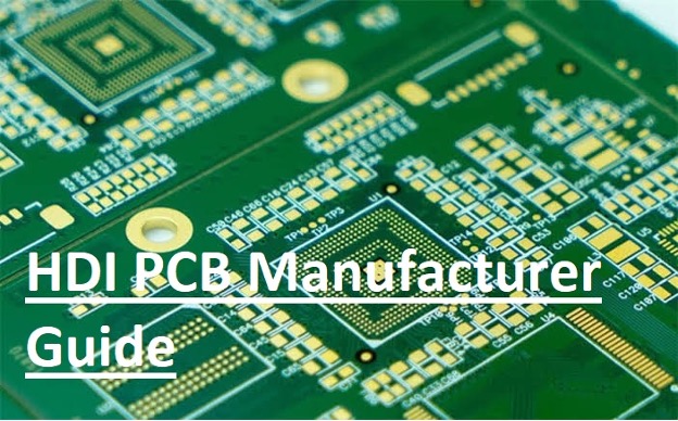
Advanced Design, Manufacturing Processes, and Quality Assurance
Modern electronic devices continue to shrink while becoming more powerful and feature-rich. Smartphones, medical equipment, automotive electronics, AI servers, industrial controllers, and communication systems all require circuit boards capable of supporting extremely dense component layouts and high-speed signal transmission. This growing demand has made HDI PCB manufacturing one of the most important technologies in the electronics industry.
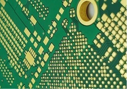
Unlike conventional multilayer boards, High-Density Interconnect (HDI) PCBs use laser-drilled microvias, blind and buried vias, fine-line circuitry, and sequential lamination to achieve significantly higher routing density within a compact footprint. These technologies enable engineers to design smaller products without sacrificing electrical performance or reliability.
However, selecting an HDI PCB manufacturer involves much more than comparing prices. Manufacturing capability, design support, material selection, quality assurance, inspection systems, and process control all directly affect product performance and long-term reliability. Poorly manufactured HDI boards may experience signal degradation, microvia failures, delamination, or reduced service life.
This guide explains how HDI PCB technology works, the manufacturing processes involved, common reliability challenges, and the key factors engineers should evaluate when choosing an experienced manufacturing partner.
Why HDI PCB Technology Matters in Modern Electronics
The Evolution of Electronic Products
Electronics have evolved dramatically over the past two decades. Designers are expected to integrate more functions into smaller products while maintaining higher processing speeds and lower power consumption. Modern systems often include:
- Fine-pitch BGAs
- High-pin-count processors
- DDR memory
- High-speed interfaces
- RF communication modules
- Multiple sensors on compact boards
Traditional multilayer PCBs often struggle to accommodate these requirements because routing space becomes increasingly limited as component density grows.
Limitations of Conventional Multilayer PCBs
Standard multilayer PCBs remain suitable for many industrial applications, but several limitations become apparent when dealing with complex designs:
- Routing congestion around dense BGAs
- Larger overall board dimensions
- Increased signal path lengths
- Higher parasitic inductance and capacitance
- Greater electromagnetic interference (EMI)
- Reduced flexibility for component placement
These constraints become particularly problematic in applications requiring high-speed data transmission or compact product dimensions.
How HDI Technology Solves These Challenges
HDI technology introduces several advanced manufacturing techniques that dramatically improve PCB performance:
- Laser-drilled microvias
- Blind and buried vias
- Fine line and spacing technology
- Sequential buildup lamination
- Copper-filled via-in-pad structures
Together, these features allow designers to increase routing density, reduce signal path lengths, improve impedance control, and optimize overall electrical performance.
What Is an HDI PCB?
High Density Interconnect (HDI) PCB s are advanced printed circuit boards designed to provide substantially higher wiring density than conventional multilayer boards.
According to IPC standards, HDI technology typically incorporates one or more of the following:
- Laser-drilled microvias
- Blind vias
- Buried vias
- Sequential lamination
- Fine conductor geometry
- Via-in-pad technology
Instead of relying solely on mechanically drilled through-holes, HDI boards use laser drilling to create extremely small interconnections between adjacent layers. This enables far greater routing flexibility while reducing board size.
Core HDI Technologies
Laser Microvias
Microvias are tiny laser-drilled holes, usually less than 150 μm in diameter, that connect adjacent copper layers. Their short electrical path improves signal integrity while minimizing parasitic effects.
Blind and Buried Vias
Blind vias connect an outer layer to an inner layer without passing completely through the board, while buried vias remain entirely within internal layers. These structures free valuable routing space on outer layers.
Via-in-Pad
Via-in-pad technology places vias directly beneath component pads, making it possible to route fine-pitch BGAs that would otherwise be impossible using conventional techniques.
Copper-Filled Microvias
Copper-filled vias improve thermal conductivity, enhance structural integrity, and provide flat surfaces for BGA assembly.
HDI PCB vs Standard Multilayer PCB
| Feature | HDI PCB | Standard PCB |
| Via Type | Microvias, blind, buried | Through-hole only |
| Routing Density | Very High | Moderate |
| Signal Integrity | Excellent | Good |
| Board Size | Smaller | Larger |
| Manufacturing Complexity | High | Moderate |
| Cost | Higher | Lower |
Although HDI fabrication is more complex, the resulting improvements in electrical performance and miniaturization often justify the additional investment.
HDI PCB Classifications and Stack-Up Structures
HDI boards are commonly classified according to their interconnection structures.
Type I HDI
Type I designs incorporate a single layer of laser microvias together with conventional through holes. They are ideal for entry-level HDI applications where moderate routing density is sufficient.
Type II HDI
Type II boards introduce blind and buried vias, allowing significantly greater routing flexibility and improved layer utilization.
Type III HDI
Type III represents advanced HDI technology using multiple sequential buildup layers and stacked microvias to achieve extremely high interconnect density.
Common HDI Stack-Up Configurations
1+N+1
One buildup layer on each side of the PCB core provides a cost-effective solution for many commercial electronics.
2+N+2
Additional buildup layers support higher routing density and simplify fine-pitch BGA breakout.
3+N+3
Used in advanced networking equipment, AI hardware, aerospace electronics, and high-performance computing systems requiring maximum routing capacity.
HDI PCB Design Fundamentals
Design quality directly affects manufacturing yield, electrical performance, and long-term reliability.
Key design considerations include:
Fine-Pitch BGA Fanout
Proper fanout strategies prevent routing congestion while maximizing escape routing efficiency.
Controlled Impedance
Modern high-speed interfaces require carefully controlled trace geometry to maintain signal integrity and reduce reflections.
Differential Pair Routing
High-speed differential signals should maintain:
- Consistent spacing
- Equal trace lengths
- Minimal discontinuities
Return Path Optimization
Continuous reference planes minimize loop inductance and reduce electromagnetic emissions.
Power Distribution Networks
Well-designed power planes reduce voltage fluctuations while improving transient response.
Design for Manufacturability (DFM)
Successful HDI designs account for manufacturing tolerances from the beginning. Close collaboration between PCB designers and manufacturers reduces production risks while improving overall yield.
Materials Used in HDI PCB Manufacturing
Material selection significantly influences thermal stability, electrical performance, and long-term reliability.
Common materials include:
- Standard FR-4
- High-Tg FR-4
- Halogen-free laminates
- Low-loss high-speed materials
- Low Dk / Low Df laminates
When selecting materials, engineers evaluate several important parameters:
| Property | Importance |
| Tg | Glass transition temperature |
| Td | Thermal decomposition resistance |
| CTE | Thermal expansion |
| Dk | Dielectric constant |
| Df | Dissipation factor |
| CAF Resistance | Long-term insulation reliability |
Low-loss materials become particularly important for 5G communication equipment, RF circuits, and high-speed computing systems where insertion loss must be minimized.
HDI PCB Manufacturing Process
Producing an HDI PCB requires significantly more precision than conventional PCB fabrication.
A typical manufacturing workflow includes:
- Inner-layer imaging
- Inner-layer etching
- Core lamination
- Laser microvia drilling
- Desmear processing
- Copper plating
- Sequential lamination
- Via filling
- Outer-layer imaging
- Solder mask application
- Surface finish
- Electrical testing
- Final inspection
Among these steps, laser drilling and copper plating are particularly critical because microvia quality directly determines long-term reliability.
Manufacturers must carefully control drilling accuracy, plating thickness, layer registration, and thermal processing throughout production. Even small variations can affect impedance consistency or create reliability concerns during thermal cycling.
HDI PCB Manufacturer Guide
Advanced HDI Manufacturing Capabilities
As electronic products become more sophisticated, manufacturers must continually improve their fabrication capabilities to meet increasingly demanding design requirements. A capable HDI PCB manufacturer invests in advanced equipment, automated inspection systems, and experienced engineering teams to consistently produce reliable, high-density circuit boards.
When evaluating a manufacturer, consider the following technical capabilities:
| Manufacturing Capability | Typical Advanced Capability | Why It Matters |
| Minimum line width/spacing | 2.5 mil / 2.5 mil | Supports dense routing and fine-pitch components |
| Laser microvias | Blind, buried, stacked, staggered | Enables compact HDI designs |
| Layer count | Up to 50 layers | Supports complex networking and computing systems |
| Aspect ratio | Up to 30:1 | Improves drilling capability for thick boards |
| Controlled impedance | ±5% tolerance | Ensures high-speed signal integrity |
| Rigid-flex capability | Up to 20 layers | Ideal for compact electronic products |
| Flexible PCB capability | Up to 10 layers | Reduces connectors and improves reliability |
In addition to fabrication capabilities, surface finish options are equally important. Common finishes include:
- ENIG (Electroless Nickel Immersion Gold): Excellent solderability and corrosion resistance.
- ENEPIG (Electroless Nickel Electroless Palladium Immersion Gold): Preferred for wire bonding and mixed assembly.
- Hard Gold: Offers superior wear resistance for edge connectors and high-cycle applications.
These capabilities provide engineers with greater design flexibility while ensuring long-term product reliability.
HDI PCB Assembly and Inspection
Fabricating an HDI PCB is only one part of the manufacturing process. Precision assembly is equally important because today’s HDI boards often incorporate extremely small components with tight placement tolerances.
Common HDI Assembly Challenges
Modern HDI assemblies frequently include:
- Fine-pitch BGA packages
- QFN devices
- FPGA packages
- 01005 passive components
- High-pin-count processors
- RF modules
Each of these components requires highly accurate solder paste deposition, component placement, and controlled reflow profiles.
Automated Optical Inspection (AOI)
AOI systems automatically inspect every assembled board for:
- Missing components
- Incorrect polarity
- Misalignment
- Solder bridges
- Tombstoning
- Insufficient solder
Automated inspection significantly improves manufacturing consistency while reducing manual inspection errors.
X-Ray Inspection
Many solder joints, particularly beneath BGA and QFN packages, cannot be inspected visually.
High-resolution X-ray systems verify:
- Hidden solder joints
- Voids
- Head-in-pillow defects
- Open connections
- Short circuits
- BGA alignment
For mission-critical electronics, many manufacturers perform 100% X-ray inspection of BGA assemblies to ensure defect-free solder joints.
Functional Testing
Inspection alone cannot guarantee electrical performance. Manufacturers typically combine visual inspection with electrical testing methods such as:
- In-Circuit Testing (ICT)
- Flying Probe Testing
- Functional Testing
- Boundary Scan (JTAG)
These tests confirm that the finished assembly performs according to design specifications before shipment.
Quality Assurance and Reliability Validation
Reliable HDI PCB production depends on strict quality management throughout every manufacturing stage.
Industry Standards
Leading manufacturers comply with internationally recognized standards, including:
- IPC Class 2
- IPC Class 3
- ISO 9001 Quality Management
- ISO 13485 (Medical Devices)
Compliance with these standards demonstrates that manufacturing processes are documented, repeatable, and continuously monitored.
Reliability Testing
To ensure long-term performance, HDI PCBs undergo extensive validation, including:
- Thermal cycling
- Solderability testing
- Cross-section analysis
- Impedance verification
- Copper thickness measurement
- Microvia reliability testing
- Environmental stress testing
Cross-sectional analysis is particularly valuable because it allows engineers to examine plated holes, copper distribution, and laminate integrity under a microscope.
Common Reliability Challenges in HDI PCB Production
Although HDI technology provides exceptional electrical performance, manufacturing defects can significantly reduce reliability if process controls are inadequate.
Microvia Cracking
Repeated thermal expansion and contraction can cause microvias to crack, leading to intermittent electrical failures.
Copper Fatigue
Mechanical stress and thermal cycling may eventually weaken plated copper inside vias, particularly in stacked microvia structures.
Delamination
Poor lamination processes or moisture absorption can cause internal layers to separate, reducing structural integrity.
CAF (Conductive Anodic Filament) Formation
Moisture combined with electrical bias can create conductive paths within the laminate, causing insulation failures.
Registration Errors
Misalignment during sequential lamination may reduce annular rings or create open circuits.
Thermal Stress
High-power electronics place continuous stress on PCB materials. Proper material selection and thermal management help reduce these risks.
Experienced manufacturers minimize these issues through process optimization, statistical process control (SPC), automated inspection, and comprehensive reliability testing.
Applications of HDI PCB Technology
HDI PCBs are widely used across industries where compact size, high performance, and reliability are essential.
5G Infrastructure
Base stations, RF modules, and high-frequency communication equipment rely on HDI technology for controlled impedance and reduced signal loss.
Medical Electronics
Portable diagnostic equipment, patient monitoring devices, and surgical instruments require compact, highly reliable PCBs that meet strict quality standards.
Automotive Electronics
Advanced Driver Assistance Systems (ADAS), infotainment systems, radar modules, and electric vehicle control units all benefit from HDI technology.
AI Servers and Data Centers
High-speed processors, memory modules, and networking hardware require multilayer HDI boards capable of supporting extremely dense routing.
Aerospace and Defense
Mission-critical avionics and defense electronics depend on robust HDI designs capable of withstanding harsh operating environments.
Industrial Automation
Industrial control systems, robotics, and factory automation equipment require reliable HDI boards for continuous operation.
Consumer Electronics
Smartphones, tablets, laptops, wearable devices, and gaming systems all use HDI PCBs to maximize functionality within limited space.
How to Choose the Right HDI PCB Manufacturer
Choosing the right manufacturing partner is one of the most important decisions in any electronics project.
Before placing an order, evaluate the following areas:
Engineering Support
A strong engineering team should provide:
- Design for Manufacturability (DFM) review
- Stack-up recommendations
- Material selection guidance
- Signal integrity consultation
- Cost optimization suggestions
Manufacturing Technology
Confirm that the manufacturer supports:
- HDI 1+N+1 through Any-Layer HDI
- Laser-drilled microvias
- Blind and buried vias
- Copper-filled via-in-pad
- Sequential lamination
Quality Systems
Look for manufacturers certified to:
- ISO 9001
- ISO 13485 (if medical products are involved)
- IPC Class 3 (for high-reliability applications)
Inspection Equipment
Reliable manufacturers should utilize:
- AOI
- X-ray inspection
- Flying probe testing
- Impedance measurement
- Cross-section analysis
Turnkey Services
Working with a manufacturer that offers fabrication, assembly, testing, and logistics under one roof simplifies project management and reduces lead time.
Conclusion
HDI PCB technology has become an essential part of modern electronics, enabling engineers to design smaller, faster, and more reliable products than ever before. Through advanced features such as laser-drilled microvias, blind and buried vias, sequential lamination, and fine-line circuitry, HDI boards overcome the limitations of conventional multilayer PCBs while improving signal integrity, power distribution, and overall system performance.
However, achieving these benefits depends heavily on selecting an experienced manufacturing partner. A reliable HDI PCB manufacturer should combine advanced fabrication technologies with comprehensive engineering support, rigorous quality assurance, precision assembly, and extensive testing capabilities. By carefully evaluating manufacturing expertise, inspection systems, material options, and quality certifications, designers can reduce production risks and ensure consistent performance from prototype development through high-volume manufacturing.
For organizations developing next-generation electronic products, partnering with an experienced manufacturer such as FastTurn PCB can provide access to advanced HDI fabrication, precision assembly, and engineering support that help transform complex PCB designs into reliable, manufacturable products while meeting today’s demanding industry standards
Frequently Asked Questions
Can HDI PCBs improve signal integrity?
Yes. HDI PCBs reduce signal path lengths, minimize parasitic inductance and capacitance, and provide better impedance control, making them well suited for high-speed digital and RF applications.
What industries use HDI PCBs?
HDI technology is widely used in telecommunications, medical electronics, automotive systems, aerospace, industrial automation, AI servers, data centers, consumer electronics, and IoT devices.
Why are laser microvias important?
Laser microvias enable higher routing density, improve electrical performance, reduce board size, and support fine-pitch BGA packages that cannot be routed efficiently using traditional through-hole vias.
Are HDI PCBs more expensive than conventional PCBs?
Generally, yes. The advanced materials, specialized equipment, and additional manufacturing steps increase production costs. However, HDI technology often reduces overall system size and improves performance, making it cost-effective for many advanced applications.
What should I look for in an HDI PCB manufacturer?
Consider manufacturing capabilities, stack-up options, material expertise, impedance control, inspection systems, certifications (such as ISO 9001 and IPC Class 3), engineering support, and experience with similar projects.