[nextpage title=”Introduction”]
The EarthWatts Platinum is the latest power supply series from Antec, and will be available in 450 W, 550 W, and 650 W versions, coming with the 80 Plus Platinum certification. This new series will reach the North American market next month; we were able to get a sample before its official release. Let’s see if the 650 W model is a good option.
The EarthWatts Platinum is manufactured by FSP.
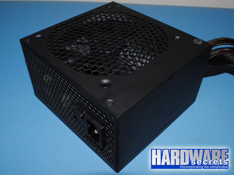
Figure 1: Antec EarthWatts Platinum 650 W power supply
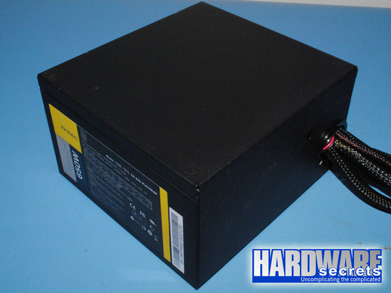
Figure 2: Antec EarthWatts Platinum 650 W power supply
The Antec EarthWatts Platinum 650 W is 5.5” (140 mm) deep, using a 120 mm ball bearing fan on its bottom (Yate Loon D12BH-12).
This unit doesn’t have a modular cabling system, and all cables use nylon sleeves that come from inside the unit. This power supply comes with the following cables:
- Main motherboard cable with a 24-pin connector, 20.5” (52 cm) long
- One cable with two ATX12V connectors that together form an EPS12V connector, 23.6” (60 cm) long
- One cable with two six/eight-pin connectors for video cards, 21.3” (54 cm) to the first connector, 5.9” (15 cm) between connectors
- One cable with three SATA power connectors, 21.3” (54 cm) to the first connector, 5.9” (15 cm) between connectors
- One cable with three SATA power connectors and one standard peripheral power connector, 21.3” (54 cm) to the first connector, 5.9” (15 cm) between connectors
- One cable with three standard peripheral power connectors and one floppy disk drive power connector, 21.3” (54 cm) to the first connector, 5.9” (15 cm) between connectors
All wires are 18 AWG wires, which is the minimum recommended gauge.
The cable configuration is fair for a 650 W power supply, with long SATA and peripheral power cables.
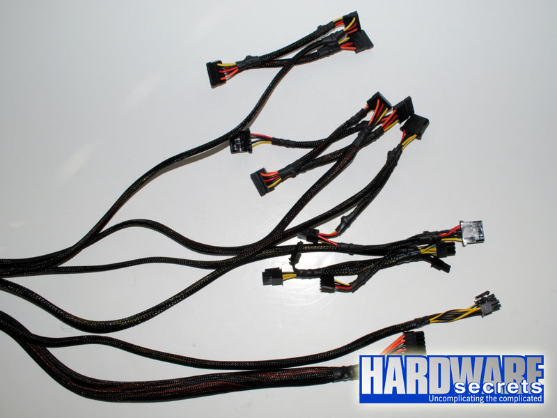
Figure 3: Cables
Let’s now take an in-depth look inside this power supply.
[nextpage title=”A Look Inside the Antec EarthWatts Platinum 650 W”]
We decided to disassemble this power supply to see what it looks like inside, how it is designed, and what components are used. Please read our “Anatomy of Switching Power Supplies” tutorial to understand how a power supply works and to compare this power supply to others.
On this page we will have an overall look, and then in the following pages we will discuss in detail the quality and ratings of the components used.

Figure 4: Top view

Figure 5: Front quarter view

Figure 6: Rear quarter view

Figure 7: The printed circuit board
[nextpage title=”Transient Filtering Stage”]
As we have mentioned in other articles and reviews, the first place we look when opening a power supply for a hint about its quality, is its filtering stage. The recommended components for this stage are two ferrite coils, two ceramic capacitors (Y capacitors, usually blue), one metalized polyester capacitor (X capacitor), and one MOV (Metal-Oxide Varistor). Very low-end power supplies use fewer components, usually removing the MOV and the first coil.
In this stage, the Antec EarthWatts Platinum 650 W power supply is flawless. It has two Y capacitors and one X capacitor more than the minimum required.
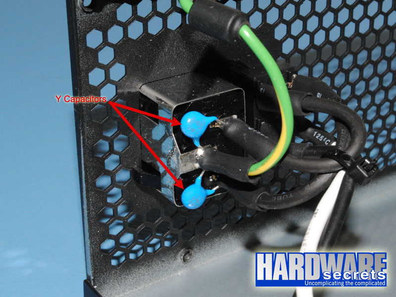
Figure 8: Transient filtering stage (part 1)
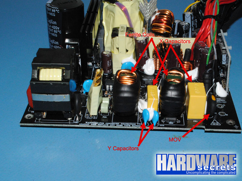
Figure 9: Transient filtering stage (part 2)
On the next page, we will have a more detailed discussion about the components used in the Antec EarthWatts Platinum 650 W.
[nextpage title=”Primary Analysis”]
On this page we will take an in-depth look at the primary stage of the Antec EarthWatts Platinum 650 W. For a better understanding, please read our “Anatomy of Switching Power Supplies” tutorial.
This power supply uses one GBU15L06 rectifying bridge, which is attached to an individual heatsink. This bridge supports up to 15 A at 115° C, so in theory, you would be able to pull up to 1,725 W from a 115 V power grid. Assuming 80% efficiency, the bridge would allow this unit to deliver up to 1,380 W without burning itself out. Of course, we are only talking about this particular component. The real limit will depend on all the components combined in this power supply.
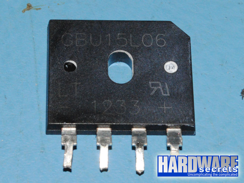
Figure 10: Rectifying bridge
The active PFC circuit uses two IPA60R125CP MOSFETs, each one capable of delivering up to 25 A at 25° C or 16 A at 100° C in continuous mode (note the difference temperature makes), or up to 82 A in pulse mode at 25° C. These transistors present a 125 mΩ resistance when turned on, a characteristic called RDS(on). The lower this number the better, meaning that the transistors will waste less power, and the power supply will achieve a higher efficiency.
The output of the active PFC circuit is filtered by a 390 µF x 420 V electrolytic capacitor from CapXon and labeled at 85° C.
In the switching section, the Antec EarthWatts Platinum 650 W uses the same unique design adopted by FSP on their 80 Plus Gold power supplies, called active clamp reset forward. The switching transistor is an SPA17N80C3 MOSFET, which is capable of delivering up to 17 A at 25° C or 11 A at 100° C in continuous mode (note the difference temperature makes), or up to 51 A at 25° C in pulse mode. This transistor presents a 290 mΩ RDS(on). A second transistor (resetting transistor) is used to turn off the switching transistor and is controlled from the secondary side. The transistor used for this function is an FQPF3N80C. This is exactly the same configuration used in the FSP Aurum Gold 700 W and the FSP Aurum CM Gold 750 W.
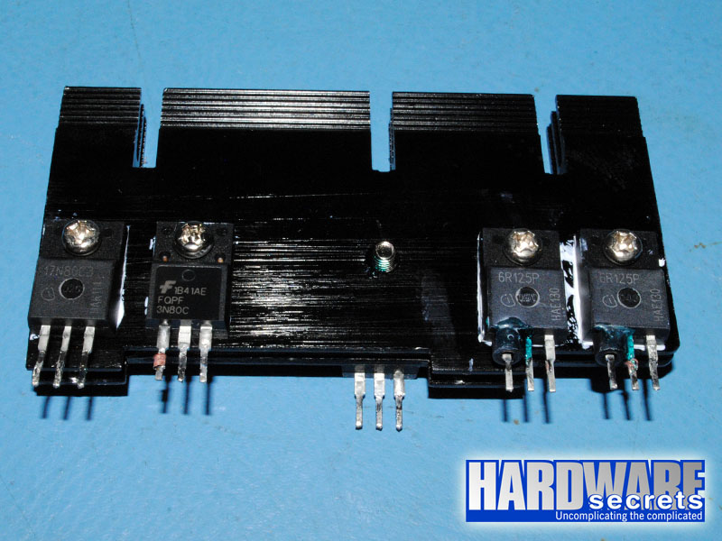
Figure 11: Switching transistors and active PFC transistors
The primary is managed by a custom-made PFC/PWM controller called FSP6600. Since this is a custom integrated circuit, no datasheet is available for it.
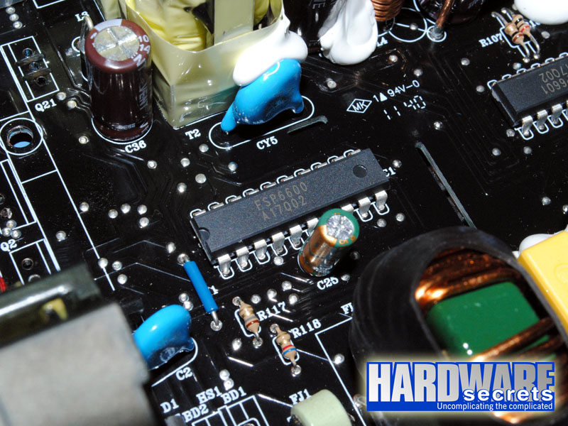
Figure 12: Active PFC/PWM controller
Let’s now take a look at the secondary of this power supply.
[nextpage title=”Secondary Analysis”]
This power supply uses a synchronous design in its secondary, meaning that the diodes were replaced with transistors in order to increase efficiency.
The +12 V output is rectified using two IRLB3036 MOSFETs, each one capable of handling up to 270 A at 25° C or up to 190 A at 100° C in continuous mode, or up to 1,100 A at 25° C in pulse mode. This translates into a maximum theoretical current of 271 A at 100° C or 3,257 W! These are the same transistors used in the FSP Aurum Gold 700 W and FSP Aurum CM Gold 750 W.

Figure 13: +12 V transistors
The +5 V and +3.3 V outputs share the same circuitry and are rectified by four IPD031N03L MOSFETs, each one supporting 90 A at 100° C in continuous mode and 400 A at 25° C in pulse mode, 3.1 mΩ RDS(on). The four transistors are located on the solder side of the printed circuit board.

Figure 14: The +5 V and +3.3 V transistors
The secondary transistors are controlled by an FSP6601, another proprietary chip from FSP.

Figure 15: Synchronous controller
The secondary is monitored by a WT7579 integrated circuit, which is manufactured exclusively for FSP. This chip supports over voltage (OVP), under voltage (UVP), overcurrent (OCP), and over temperature (OTP) protections. There are four +12 V over current protection (OCP) channels, matching the number of +12 V rails advertised by the manufacturer.

Figure 16: Monitoring circuit
Some of the electrolytic capacitors used in the secondary are Japanese, from Chemi-Con, and some are from CapXon.
[nextpage title=”Power Distribution”]
In Figure 17, you can see the power supply label containing all the power specs.
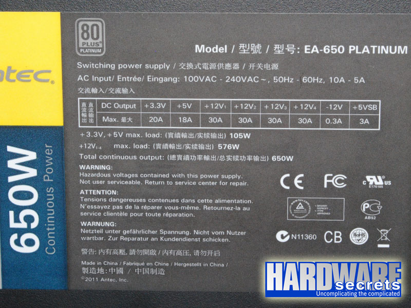
Figure 17: Power supply label
As you can see, the manufacturer lists this unit as having four +12 V rails. Analyzing the circuit, we could clearly see four “shunts” (current sensors), matching the number of rails advertised by the manufacturer, and the monitoring circuit really has four separate +12 V over current protection (OCP) channels. See Figure 18. Click here to understand more about this subject.
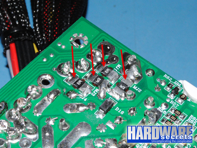
Figure 18: Shunts
The available +12 V rails are distributed like this:
- +12V1 (solid yellow wire): SATA and peripheral power connectors
- +12V2 (yellow/black wire): The ATX12V/EPS12V cable
- +12V3 (solid yellow wire): Main motherboard cable
- +12V4 (yellow/blue wire): The video card power connectors
This distribution is perfect, as it separates the CPU and the video card power cables on individual rails.
How much power can this unit really deliver? Let’s find out.
[nextpage title=”Load Tests”]
We conducted several tests with this power supply, as described in the article, “Hardware Secrets Power Supply Test Methodology.”
First we tested this power supply with five different load patterns, trying to pull around 20%, 40%, 60%, 80%, and 100% of its labeled maximum capacity (actual percentage used listed under “% Max Load”), watching the behavior of the reviewed unit und
er each load. In the table below, we list the load patterns we used and the results for each load.
If you add all the powers listed for each test, you may find a different value than what is posted under “Total” below. Since each output can have a slight variation (e.g., the +5 V output working at +5.10 V), the actual total amount of power being delivered is slightly different than the calculated value. In the “Total” row, we are using the real amount of power being delivered, as measured by our load tester.
The +12VA and +12VB inputs listed below are the two +12 V independent inputs from our load tester. During this test, the +12VA input was connected to the power supply +12V1, +12V3, and +12V4 rails, while the +12VB input was connected to the power supply +12V2 rail.
| Input | Test 1 | Test 2 | Test 3 | Test 4 | Test 5 |
| +12VA | 5 A (60 W) | 10 A (120 W) | 14.5 A (174 W) | 19 A (228 W) | 23.5 A (282 W) |
| +12VB | 5 A (60 W) | 10 A (120 W) | 14 A (168 W) | 19 A (228 W) | 23 A (276 W) |
| +5 V | 1 A (5 W) | 2 A (10 W) | 4 A (20 W) | 6 A (30 W) | 8 A (40 W) |
| +3.3 V | 1 A (3.3 W) | 2 A (6.6 W) | 4 A (13.2 W) | 6 A (19.8 W) | 8 A (26.4 W) |
| +5VSB | 1 A (5 W) | 1.5 A (7.5 W) | 2 A (10 W) | 2.5 A (12.5 W) | 3 A (15 W) |
| -12 V | 0.5 A (6 W) | 0.5 A (6 W) | 0.5 A (6 W) | 0.5 A (6 W) | 0.5 A (6 W) |
| Total | 141.6 W | 269.3 W | 393.7 W | 524.8 W | 646.6 W |
| % Max Load | 21.8% | 41.4% | 60.6% | 80.7% | 99.5% |
| Room Temp. | 45.7° C | 44.0° C | 45.3° C | 47.7° C | 49.2° C |
| PSU Temp. | 47.7° C | 45.8° C | 47.0° C | 49.6° C | 53.6° C |
| Voltage Regulation | Pass | Pass | Pass | Pass | Pass |
| Ripple and Noise | Pass | Pass | Pass | Pass | Pass |
| AC Power | 155.9 W | 290.9 W | 429.4 W | 581.8 W | 727.0 W |
| Efficiency | 90.8% | 92.6% | 91.7% | 90.2% | 88.9% |
| AC Voltage | 118.0 V | 116.9 V | 115.1 V | 113.7 V | 111.8 V |
| Power Factor | 0.970 | 0.989 | 0.997 | 0.998 | 0.998 |
| Final Result | Pass | Pass | Pass | Pass | Pass |
The Antec EarthWatts Platinum 650 W passed our tests with flying colors.
Efficiency was between 88.9% and 92.6% during our tests, matching the values promised by the 80 Plus Platinum certification. At full load the 80 Plus Platinum certification promises 89% efficiency, and we can consider that this unit reaches this level since it was only 0.1% below this level.
Voltage regulation was very good, with all voltages closer to their nominal values than required (three percent regulation), for the -12 V output on all tests and the +3.3 V output at test five (+3.18 V). These outputs were still inside the allowed range. The ATX12V specification states that positive voltages must be within 5% of their nominal values, and negative voltages must be within 10% of their nominal values.
Let’s discuss the ripple and noise levels on the next page.
[nextpage title=”Ripple and Noise Tests”]
Voltages at the power supply outputs must be as “clean” as possible, with no noise or oscillation (also known as “ripple”). The maximum ripple and noise levels allowed are 120 mV for +12 V and -12 V outputs, and 50 mV for +5 V, +3.3 V and +5VSB outputs. All values are peak-to-peak figures. We consider a power supply as being top-notch if it can produce half or less of the maximum allowed ripple and noise levels.
The Antec EarthWatts Platinum 650 W provided very low ripple and noise levels, as you can see in the table below. Noise level at -12 V was a little high, but still inside the specifications.
| Test 1 | Test 2 | Test 3 | Test 4 | Test 5 | |
| +12VA | 17.2 mV | 16.4 mV | 20.2 mV | 24.6 mV | 30.6 mV |
| +12VB | 22.0 mV | 21.8 mV | 27.6 mV | 32.8 mV | 42.4 mV |
| +5 V | 13.2 mV | 13.8 mV | 15.6 mV | 18.4 mV | 22.2 mV |
| +3.3 V | 12.4 mV | 14.8 mV | 19.6 mV | 20.2 mV | 23.2 mV |
| +5VSB | 9.8 mV | 9.8 mV | 11.6 mV | 12.6 mV | 15.2 mV |
| -12 V | 49.8 mV | 35.6 mV | 55.6 mV | 60.2 mV | 70.2 mV |
Below you can see the waveforms of the outputs during test five.

Figure 19: +12VA input from load tester during test five at 646.6 W (30.6 mV)

Figure 20: +12VB input from load tester during test five at 646.6 W (22.2 mV)

Figure 21: +5V rail during test five at 646.6 W (22.2 mV)

Figure 22: +3.3 V rail during test five at 646.6 W (23.2 mV)
Let’s see if we can pull more than 650 W from this unit.
[nextpage title=”Overload Tests”]
Below you can see the maximum we could pull from this power supply. We couldn’t pull more, as the power supply would shut down, showing that its protections are present and working fine. During this extreme configuration, noise and ripple levels were still very low. Voltages exited the three percent regulation we’ve seen before, but they were still inside the allowed range.
| Input | Overload Test |
| +12VA | 30 A (360 W) |
| +12VB | 30 A (360 W) |
| +5 V | 8 A (40 W) |
| +3.3 V | 8 A (26.4 W) |
| +5VSB | 3 A (15 W) |
| -12 V | 0.5 A (6 W) |
| Total | 776.7 W |
| % Max Load | 119.5% |
| Room Temp. | 49.9° C |
| PSU Temp. | 53.6° C |
| AC Power | 907.0 W |
| Efficiency | 85.6% |
| AC V oltage | 110.3 V |
| Power Factor | 0.998 |
[nextpage title=”Main Specifications”]
The main specifications for the Antec EarthWatts Platinum 650 W power supply include:
- Standards: NA
- Nominal labeled power: 650 W
- Measured maximum power: 776.7 W at 49.9° C
- Labeled efficiency: 93% maximum, 80 Plus Platinum certification
- Measured efficiency: Between 88.9% and 92.6% at 115 V (nominal, see complete results for actual voltage)
- Active PFC: Yes
- Modular Cabling System: No
- Motherboard Power Connectors: One 24-pin connector and two ATX12V connectors that together form an EPS12V connector
- Video Card Power Connectors: Two six/eight-pin connectors on one cable
- SATA Power Connectors: Seven on two cables
- Peripheral Power Connectors: Four on two cables
- Floppy Disk Drive Power Connectors: One
- Protections (as listed by the manufacturer): Over current (OCP), over voltage (OVP), under voltage (UVP), over power (OPP), no load (NLO), and short circuit (SCP)
- Are the above protections really available? Yes
- Warranty: Three years
- Real Manufacturer: FSP
- More Information: NA
- MSRP in the US: USD 130.00
[nextpage title=”Conclusions”]
The Antec EarthWatts Platinum 650 W proved to be an excellent power supply for the user who wants high efficiency at a mainstream wattage. During our tests, efficiency was between 88.9% and 92.6%, noise and ripple levels were extremely low, and positive voltages were within three percent of their nominal values all the time (except for the +3.3 V output when we pulled 650 W from the unit, but it was still inside the allowed range).
The suggested price of USD 130 is not absurd for an 80 Plus Platinum unit, but we hope retailers sell it for less, making it more affordable for the mainstream user.
The only point we think Antec could improve would be to require FSP to use only Japanese capacitors in this unit. On the sample we received, only half of the secondary capacitors were Japanese. The other half and the main primary electrolytic capacitor are from CapXon, which is a Taiwanese company with factories in mainland China. Also, the main primary capacitor should be a 105° C model.
Although the printed circuit board for the Antec EarthWatts Platinum 650 W is different, this unit uses the same switching design and similar components as the FSP Aurum series.
Leave a Reply