[nextpage title=”Introduction”]
The Antec High Current Gamer power supply series is comprised of 400 W, 520 W, 620 W, 750 W, and 900 W models, all with 80 Plus Bronze certification, single +12 V rail, and no modular cabling system. Let’s take a look at the 520 W model.
We’ve already reviewed the 750 W model, which is manufactured by Delta Electronics. The 520 W model, however, is manufactured by Seasonic. Therefore, they don’t share the same platform.

Figure 1: Antec High Current Gamer 520 W power supply

Figure 2: Antec High Current Gamer 520 W power supply
The Antec High Current Gamer 520 W is 6.3” (160 mm) deep, using a 135 mm dual ball bearing fan on its bottom (ADDA ADN512MB-A90).
As previously mentioned, this unit doesn’t have a modular cabling system. All cables are protected with nylon sleeves. This power supply comes with the following cables:
- Main motherboard cable with a 20/24-pin connector, 21.3” (54 cm) long
- One cable with two ATX12V connectors that together form an EPS12V connector, 25.2” (64 cm) long
- One cable with two six/eight-pin connectors for video cards, 20.9” (53 cm) to the first connector, 4.7” (12 cm) between connectors
- Two cables, each with four SATA power connectors, 22” (56 cm) to the first connector, 5.9” (15 cm) between connectors
- One cable with three standard peripheral power connectors, 22” (56 cm) to the first connector, 5.9” (15 cm) between connectors
- One cable with three standard peripheral power connectors and one floppy disk drive power connector, 22” (56 cm) to the first connector, 5.9” (15 cm) between connectors
All wires are 18 AWG, which is the minimum recommended gauge.
The cable configuration is very good for a 520 W product, with eight SATA power connectors and two video card power connectors.

Figure 3: Cables
Let’s now take an in-depth look inside this power supply.
[nextpage title=”A Look Inside the Antec High Current Gamer 520 W”]
We decided to disassemble this power supply to see what it looks like inside, how it is designed, and what components are used. Please read our Anatomy of Switching Power Supplies tutorial to understand how a power supply works and to compare this power supply to others.
On this page we will have an overall look, and then in the following pages we will discuss in detail the quality and ratings of the components used.
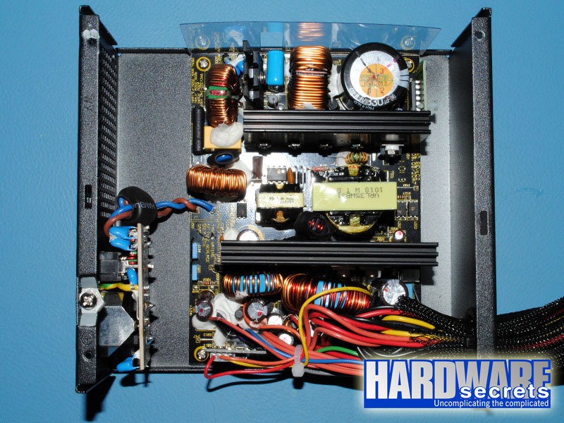
Figure 4: Top view

Figure 5: Front quarter view
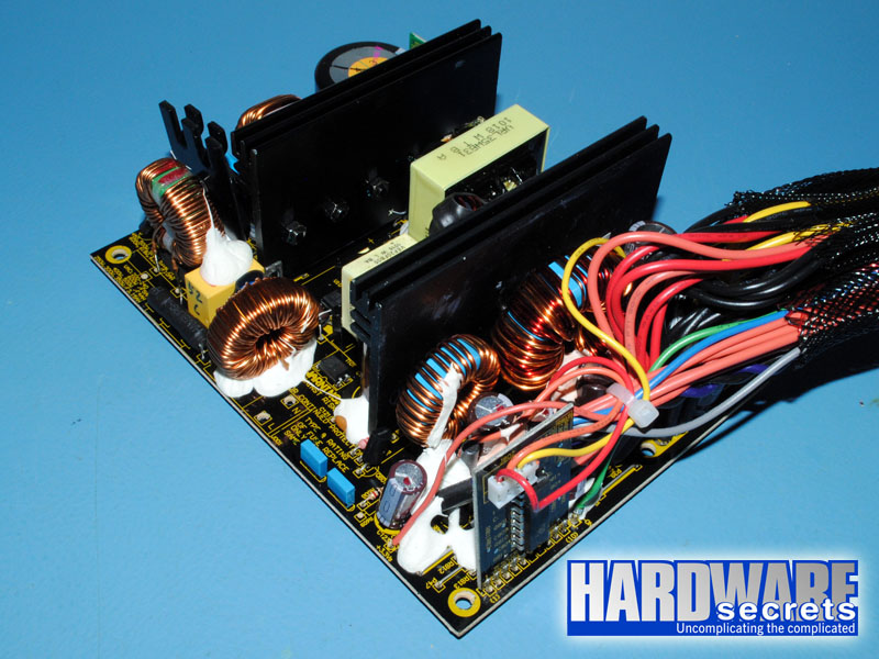
Figure 6: Rear quarter view
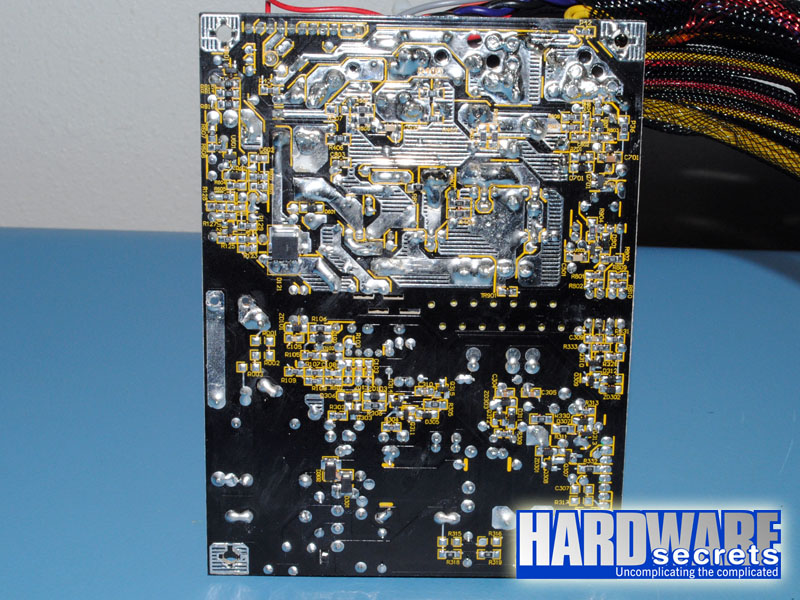
Figure 7: The printed circuit board
[nextpage title=”Transient Filtering Stage”]
As we have mentioned in other articles and reviews, the first place we look when opening a power supply for a hint about its quality, is its filtering stage. The recommended components for this stage are two ferrite coils, two ceramic capacitors (Y capacitors, usually blue), one metalized polyester capacitor (X capacitor), and one MOV (Metal-Oxide Varistor). Very low-end power supplies use fewer components, usually removing the MOV and the first coil.
In this stage, this power supply is flawless, with one X capacitor, four Y capacitors, and one ferrite coil more than the minimum required.

Figure 8: Transient filtering stage (part 1)

Figure 9: Transient filtering stage (part 2)
On the next page, we will have a more detailed discussion about the components used in the Antec High Current Gamer 520 W.
[nextpage title=”Primary Analysis”]
On this page we will take an in-depth look at the primary stage of the Antec High Current Gamer 520 W. For a better understanding, please read our Anatomy of Switching Power Supplies tutorial.
This power supply uses one GBU806 rectifying bridge, attached to an individual heatsink. This bridge supports up to 8 A at 100° C, so in theory, you would be able to pull up to 920 W from a 115 V power grid. Assuming 80% efficiency, the bridge would allow this unit to deliver up to 736 W without burning itself out. Of course, we are only talking about these particular components. The real limit will depend on all the components combined in this power supply.

Figure 10: Rectifying bridge
The active PFC circuit uses two FDP18N50 MOSFETs, each supporting up to 18 A at 25° C or 10.8 A at 100&d
eg; C in continuous mode (note the difference temperature makes), or 72 A at 25° C in pulse mode. These transistors present a 265 mΩ resistance when turned on, a characteristic called RDS(on). The lower the number the better, meaning that the transistor will waste less power, and the power supply will have a higher efficiency.

Figure 11: One of the switching transistors, active PFC diode, and active PFC transistors
The output of the active PFC circuit is filtered by a Japanese capacitor, from Chemi-Con, labeled at 85° C.
In the switching section, another two FDP18N50 MOSFETs are used in the traditional two-transistor forward configuration. The specifications for these transistors were discussed above.

Figure 12: The other switching transistor
The primary is controlled by an ICE1CS02 active PFC/PWM combo controller.

Figure 13: Active PFC/PWM combo controller
Let’s now take a look at the secondary of this power supply.
[nextpage title=”Secondary Analysis”]
The Antec High Current Gamer 520 W uses a regular design in its secondary, with Schottky rectifiers.
The maximum theoretical current each line can deliver is given by the formula I / (1 – D) where D is the duty cycle used and I is the maximum current supported by the rectifying diode. As an exercise, we can assume a duty cycle of 30 percent.
The +12 V output uses two SBR30A50CT Schottky rectifiers (30 A, 15 A per internal diode at 110° C, 0.55 V maximum voltage drop). This gives us a maximum theoretical current of 43 A or 514 W for the +12 V output.
The +5 V output uses another SBR30A50CT Schottky rectifier. This gives us a maximum theoretical current of 21 A or 107 W for the +5 V output.
The +3.3 V output uses an SBR40U45CT Schottky rectifier (40 A, 20 A per internal diode at 110° C, 0.52 V maximum voltage drop). This gives us a maximum theoretical current of 29 A or 94 W for the +3.3 V output.

Figure 14: The +12 V, +3.3 V, and +5VSB rectifiers

Figure 15: The +5 V and +12 V rectifiers
This power supply uses a PS223 monitoring integrated circuit, which supports over voltage (OVP), under voltage (UVP), over current (OCP), and over temperature (OTP) protections. This chip offers two +12 V channels, but the manufacturer decided to use only one of them to make this unit have a single +12 V rail.

Figure 16: Monitoring circuit
The electrolytic capacitors that filter the outputs are also Japanese, from Chemi-Con.
[nextpage title=”Power Distribution”]
In Figure 17, you can see the power supply label containing all the power specs.

Figure 17: Power supply label
This power supply uses a single-rail design, so there is not much to talk about here.
How much power can this unit really deliver? Let’s find out.
[nextpage title=”Load Tests”]
We conducted several tests with this power supply, as described in the article Hardware Secrets Power Supply Test Methodology.
First we tested this power supply with five different load patterns, trying to pull around 20%, 40%, 60%, 80%, and 100% of its labeled maximum capacity (actual percentage used listed under “% Max Load”), watching the behavior of the reviewed unit under each load. In the table below, we list the load patterns we used and the results for each load.
If you add all the powers listed for each test, you may find a different value than what is posted under “Total” below. Since each output can have a slight variation (e.g., the +5 V output working at +5.10 V), the actual total amount of power being delivered is slightly different than the calculated value. In the “Total” row, we are using the real amount of power being delivered, as measured by our load tester.
The +12VA and +12VB inputs listed below are the two +12 V independent inputs from our load tester. During this test, both inputs were connected to the power supply’s single +12 V rail.
| Input | Test 1 | Test 2 | Test 3 | Test 4 | Test 5 |
| +12VA | 4 A (48 W) | 7.5 A (90 W) | 11 A (132 W) | 14.5 A (174 W) | 18 A (216 W) |
| +12VB | 4 A (48 W) | 7.5 A (90 W) | 11 A (132 W) | 14.5 A (174 W) | 18 A (216 W) |
| +5 V | 1 A (5 W) | 2 A (10 W) | 4 A (20 W) | 6 A (30 W) | 8 A (40 W) |
| +3.3 V | 1 A (3.3 W) | 2 A (6.6 W) | 4 A (13.2 W) | 6 A (19.8 W) | 8 A (26.4 W) |
| +5VSB | 1 A (5 W) | 1 A (5 W) | 1.5 A (7.5 W) | 2 A (10 W) | 2.5 A (12.5 W) |
| -12 V | 0.5 A (6 W) | 0.5 A (6 W) | 0.5 A (6 W) | 0.5 A (6 W) | 0.5 A (6 W) |
| Total | 104.4 W | 209.8 W | 313.8 W | 416.1 W | 520.4 W |
| % Max Load | 20.1% | 40.3% | 60.3% | 80.0% | 100.1% |
| Room Temp. | 44.8° C | 43.9° C | 44.0° C | 45.2° C | 47.2° C |
| PSU Temp. | 45.5° C | 45.3° C | 45.4° C
| 46.0° C | 47.0° C |
| Voltage Regulation | Pass | Pass | Pass | Pass | Pass |
| Ripple and Noise | Pass | Pass | Pass | Pass | Pass |
| AC Power | 123.5 W | 243.6 W | 366.8 W | 495.3 W | 632.0 W |
| Efficiency | 84.5% | 86.1% | 85.6% | 84.0% | 82.3% |
| AC Voltage | 115.5 V | 114.0 V | 112.7 V | 111.5 V | 109.3 V |
| Power Factor | 0.995 | 0.995 | 0.996 | 0.996 | 0.995 |
| Final Result | Pass | Pass | Pass | Pass | Pass |
The Antec High Current Gamer 520 W can really deliver its labeled wattage at high temperatures.
Efficiency was between 82.3% and 86.1%, which is terrific, as time after time we see 80 Plus Bronze power supplies that aren’t capable of reaching 82% efficiency at full load at high temperatures, which didn’t happen with the reviewed unit.
Voltages were closer to their nominal values (3% regulation) during all tests, which is great. The ATX12V specification states that positive voltages must be within 5% of their nominal values, and negative voltages must be within 10% of their nominal values.
Let’s discuss the ripple and noise levels on the next page.
[nextpage title=”Ripple and Noise Tests”]
Voltages at the power supply outputs must be as “clean” as possible, with no noise or oscillation (also known as “ripple”). The maximum ripple and noise levels allowed are 120 mV for +12 V and -12 V outputs, and 50 mV for +5 V, +3.3 V and +5VSB outputs. All values are peak-to-peak figures. We consider a power supply as being top-notch if it can produce half or less of the maximum allowed ripple and noise levels.
The Antec High Current Gamer 520 W provided really low ripple and noise levels, as you can see in the table below.
| Input | Test 1 | Test 2 | Test 3 | Test 4 | Test 5 |
| +12VA | 7.2 mV | 8.4 mV | 10.2 mV | 13.4 mV | 21.8 mV |
| +12VB | 7.6 mV | 8.8 mV | 11.0 mV | 24.4 mV | 22.8 mV |
| +5 V | 8.2 mV | 8.2 mV | 9.2 mV | 9.8 mV | 11.6 mV |
| +3.3 V | 8.4 mV | 10.4 mV | 11.8 mV | 13.4 mV | 15.6 mV |
| +5VSB | 10.2 mV | 11.0 mV | 13.4 mV | 15.8 mV | 17.6 mV |
| -12 V | 11.8 mV | 13.6 mV | 16.0 mV | 17.8 mV | 21.2 mV |
Below you can see the waveforms of the outputs during test five.

Figure 18: +12VA input from load tester during test five at 520.4 W (21.8 mV)

Figure 19: +12VB input from load tester during test five at 520.4 W (22.8 mV)

Figure 20: +5V rail during test five at 520.4 W (11.6 mV)

Figure 21: +3.3 V rail during test five at 520.4 W (15.6 mV)
Let’s see if we can pull more than 520 W from this unit.
[nextpage title=”Overload Tests”]
Below you can see the maximum we could pull from this power supply. We couldn’t pull more than that because the power supply shut down, showing that its protections were working well. During this test, all voltages were still inside the tighter 3% regulation, and ripple and noise levels were still very low.
| Input | Overload Test |
| +12VA | 22 A (264 W) |
| +12VB | 22 A (264 W) |
| +5 V | 10 A (50 W) |
| +3.3 V | 10 A (33 W) |
| +5VSB | 3 A (15 W) |
| -12 V | 0.5 A (6 W) |
| Total | 633.6 W |
| % Max Load | 121.8% |
| Room Temp. | 48.6° C |
| PSU Temp. | 50.1° C |
| AC Power | 797.0 W |
| Efficiency | 79.5% |
| AC Voltage | 106.5 V |
| Power Factor | 0.993 |
[nextpage title=”Main Specifications”]
The main specifications for the Antec High Current Gamer 520 W power supply include:
- Standards: ATX12V 2.3 and EPS12V 2.91
- Nominal labeled power: 520 W
- Measured maximum power: 633.6 W at 48.6° C ambient
- Labeled efficiency: Up to 88%, 80 Plus Bronze certification
- Measured efficiency: Between 82.3% and 86.1%, at 115 V (nominal, see complete results for actual voltage)
- Active PFC: Yes
- Modular Cabling System: No
- Motherboard Power Connectors: One 24-pin connector and two ATX12V connectors that together form an EPS12V connector
- Video Card Power Connectors: Two six/eight-pin connectors on the same cable
- SATA Power Connectors: Eight on two cables
- Peripheral Power Connectors: Six on two cables
- Floppy Disk Drive Power Connectors: One
- Protections (as listed by the manufacturer): Over voltage (OVP), over current (OCP), over power (OPP), and short-circuit (SCP) protections
- Are the above protections really available? Yes. The power supply also supports under voltage protections (UVP).
- Warranty: Three years
- More Information: https://www.antec.com
- Average Price in the US*: USD 79.00
* Researched at Newegg.com on the day we published this review.
[nextpage title=”Conclusions”]
The Antec High Current Gamer 520 W is a terrific option for the user who is looking for an affordable high-quality power supply. It can really deliver its labeled power at high temperatures, its voltages are closer to their nominal values than required (3% voltage regulation), it has very low ripple and noise levels, and efficiency is high, between 82% and 86%.
The price is fair, but of course the unit would be even better if it cost less.
Keep in mind that several power supplies with the 80 Plus Bronze certification can’t deliver 82% efficiency at high temperatures, making the Antec High Current Gamer 520 W stand out in the crowd.
Leave a Reply