
All Celeron Models
Celeron E1000 Series (Dual-Core)
Contents
Since its launch, in April, 1998, Intel Celeron processor has been going through some changes. The name Celeron is used by Intel to denominate its low cost line of processors. In fact, Celeron is an economic version of Intel top processors. In other words, Celeron is a simplified version of Pentium II, Pentium III, Pentium 4 or Core 2 Duo, with some of its features being reduced or removed. Celeron models already launched and top processors in which they are based on are listed below:
| Model | Codename | Based on | Cores | L1 Cache |
| Celeron SEPP | Convington | Pentium IIDeschutes core | 1 | 32 KB |
| Celeron A | Mendocino | Pentium II Deschutes core | 1 | 32 KB |
| Celeron PPGA | Mendocino | Pentium II Deschutes core | 1 | 32 KB |
| Celeron Coppermine | Coppermine | Pentium III Coppermine core | 1 | 32 KB |
| Celeron Tualatin | Tualatin | Pentium IIITualatin core | 1 | 32 KB |
| Celeron Willamette | Willamette | Pentium 4 Willamette core | 1 | 8 KB |
| Celeron Northwood | Northwood | Pentium 4Northwood core | 1 | 8 KB |
| Celeron D | Prescott | Pentium 4 Prescott core | 1 | 16 KB |
| Celeron 400 Series | Conroe-L | Core 2 Duo | 1 | 64 KB |
| Celeron E1000 Series | Allendale | Core 2 Duo | 2 | 64 KB |
| Celeron E3000 Series | Penryn | Core 2 Duo | 2 | 64 KB |
| Model | L2 Cache | Technology | External Bus | Socket |
| Celeron SEPP | – | 0.25 µm | 66 MHz | Slot 1 |
| Celeron A | 128 KB | 0.25 µm | 66 MHz | Slot 1 |
| Celeron PPGA | 128 KB | 0.25 µm or 0.18 µm
| 66 MHz | Socket 370 |
| Celeron Coppermine | 128 KB | 0.18 µm | 66MHz or 100MHz | Socket 370 |
| Celeron Tualatin | 256 KB | 0.13 µm | 100 MHz | Socket 370 |
| Celeron Willamette | 128 KB | 0.18 µm | 400 MHz | Socket 478 |
| Celeron Northwood | 128 KB | 0.13 µm | 400 MHz | Socket 478 |
| Celeron D | 256 KB | 90 nm or 65 nm | 533 MHz | Socket 478 or Socket LGA775 |
| Celeron 400 Series | 512 KB | 65 nm | 800 MHz | Socket LGA775 |
| Celeron E1000 Series | 512 KB | 65 nm | 800 MHz | Socket LGA775 |
| Celeron E3000 Series | 1 MB | 45 nm | 800 MHz | Socket LGA775 |
Celeron distinguishes itself from Pentium II, Pentium III, Pentium 4 or Core 2 Duo basically in three aspects:
- L2 memory cache size
- Internal clock
- External bus clock
Because of these differences Celeron is cheaper and of low-performance, compared to the Pentium II, Pentium III, Pentium 4 and Core 2 Duo processors, thus it fits well to domestic users market or to those who don’t need great power in the computer.
The first Celeron processor to be launched was an economic version of Pentium II Deschutes core. It had 32KB of L1 cache, no L2 cache, MMX technology, worked externally with 66 MHz, and was found in a printed circuit board called SEPP (Single Edge Processor Package), which was connected to the slot 1 motherboard, and was available at speeds of 266 MHz and 300 MHz.
The motherboard used by this Celeron version was the same used by the Pentium II and first Pentium III processors.
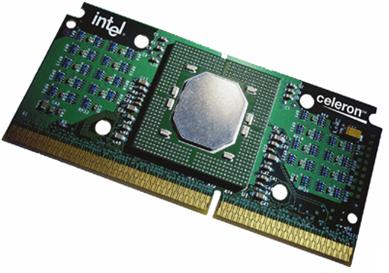
Figure 1: Celeron processor with SEPP package.
Main features of Celeron SEPP were:
- Based on Pentium II with Deschutes core
- Manufacturing process: 0.25 μm
- L1 cache: 32 KB total, 16 KB for instructions and 16 KB for data
- L2 cache: not available (0 KB)
- External clock rate: 66 MHz
- Packaging: SEPP
- Socket: Slot 1
Available models of SEPP Celeron are listed on the chart below. TDP stands for Thermal Design Power and indicates the CPU maximum thermal dissipation.
| Model | Internal Clock | Voltage | TDP |
| SL2YN | 266 MHz | 2 V | 16.59 W |
| SL2QG | 266 MHz | 2 V | 16.59 W |
| SL2SY | 266 MHz | 2 V | 16.59 W |
| SL2TR | 266 MHz | 2 V | 16.59 W |
| SL2X8 | 300 MHz | 2 V | 18.48 W |
| SL2Y2 | 300 MHz | 2 V | 18.48 W |
| SL27Z | 300 MHz | 2 V | 18.48 W |
| SL2YP | 300 MHz | 2 V | 18.48 W |
| SL2Z7 | 300 MHz | 2 V | 18.48 W |
The original Celeron was terrible. Because of no L2 cache present, its performance was less than tolerable. Thus, Intel decided to launch Celeron A, which was different from the original Celeron on its L2 cache with 128KB running at the processor speed. Actually, Celeron A was the first processor for PCs to have a L2 cache integrated in the processor.
The first version of Celeron A worked with a clock of 300 MHz. In order to differentiate from the original Celeron of 300 MHz (with no L2 cache), Intel added the letter “A” after the number. Therefore, the Celeron A 300MHz version is known as 300A.

Figure 2: Detail of the Celeron 300A marking, with 128KB on-die L2 cache.
Main features of Celeron A were:
- Based on Pentium II with Deschutes core
- Manufacturing process: 0.25 μm
- L1 cache: 32 KB total, 16 KB for instructions and 16 KB for data
- L2 cache: 128 KB
- External clock rate: 66 MHz
- Packaging: SEPP
- Socket: Slot 1
Available models of Celeron A are listed on the chart below. TDP stands for Thermal Design Power and indicates the CPU maximum thermal dissipation.
| Model | Internal Clock | Voltage | TDP |
| SL2WM | 300 MHz | 2 V | 19.05 W |
| SL32A | 300 MHz | 2 V | 19.05 W |
| SL32B | 333 MHz | 2 V | 20.94 W |
| SL2WN | 333 MHz | 2 V | 20.94 W |
| SL376 | 366 MHz | 2 V | 21.7 W |
| SL37Q | 366 MHz | 2 V | 21.7 W |
| SL37V | 400 MHz | 2 V | 23.7 W |
| SL39Z | 400 MHz | 2 V | 23.7 W |
As of the launch of Pentiu
m II, Intel started to produce its processors in the form of cartridge instead of sockets. This was the way found by Intel to transfer L2 cache, which was located on the motherboard, to the inside of the processor. In fact, L2 cache was not built-in the processor, but soldered on the same printed circuit board of the processor.
Intel had already tried before to bring L2 cache to the inside of the processor with Pentium Pro. The problem was that this solution was expensive, since there were two cores installed in the same package: one with the Pentium Pro processor and the other with 256 KB, 512 MB or 1 MB of L2 cache.
The cartridge idea didn’t work out and, in August, 1998, Intel started to produce its processors using sockets once again. The processors based on cartridge were expensive because they demanded retention mechanisms and bigger and more elaborated coolers.
Celeron PPGA was a Celeron A model developed to be installed in a socket instead of a slot. It had PPGA packaging and was installed in socket 370 motherboards. Celeron PPGA was also based in Pentium II Deschutes core processor and could be found at speeds of 300 MHz, 333 MHz, 366 MHz, 400 MHz, 433 MHz, 466 MHz, 500 MHz and 533 MHz.
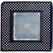
Figure 3: Celeron A with PPGA package.
Celeron PPGA can be installed in slot 1 motherboards through an adapter board, presented in Figure 4.
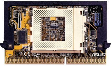
Figure 4: Adaptor board to install the Celeron PPGA on a slot 1 motherboard.
Main features of Celeron PPGA were:
- Based on Pentium II with Deschutes core
- Manufacturing process: 0.25 μm or 0.18 μm
- L1 cache: 32 KB total, 16 KB for instructions and 16 KB for data
- L2 cache: 128 KB
- External clock rate: 66 MHz
- Packaging: PPGA
- Socket: Socket 370
Available models of Celeron PPGA are listed on the chart below. TDP stands for Thermal Design Power and indicates the CPU maximum thermal dissipation.
| Model | Internal Clock | Voltage | TDP | Technology |
| SL36A | 300 MHz | 2 V | 19.05 W | 0.18 µm |
| SL35Q | 300 MHz | 2 V | 19.05 W | 0.18 µm |
| SL35R | 333 MHz | 2 V | 20.94 W | 0.25 µm |
| SL36B | 333 MHz | 2 V | 20.94 W | 0.25 µm |
| SL35S | 366 MHz | 2 V | 21.7 W | 0.25 µm |
| SL36C | 366 MHz | 2 V | 21.7 W | 0.25 µm |
| SL37X | 400 MHz | 2 V | 23.7 W | 0.25 µm |
| SL3A2 | 400 MHz | 2 V | 23.7 W | 0.25 µm |
| SL3BA | 433 MHz | 2 V | 24.1 W | 0.25 µm |
| SL3BS | 433 MHz | 2 V | 24.1 W | 0.25 µm |
| SL3EH | 466 MHz | 2 V | 25.7 W | 0.25 µm |
| SL3FL | 466 MHz | 2 V | 25.7 W | 0.25 µm |
| SL3LQ | 500 MHz | 2 V | 27.2 W | 0.25 µm |
| SL3FZ | 533 MHz | 2 V | 28.3 W | 0.25 µm |
| SL3PZ | 533 MHz | 2 V | 28.3 W | 0.25 µm |
Celeron Coppermine was based on Pentium III Coppermine core architecture and had approximately 28 millions of transistors. This was a huge figure, since Celeron SEPP had 7.5 million transistors and Celeron A had only 19 million. This increase in the number of transistors is due to the production technology used on Celeron Coppermine, which was of 0.18µm (the previous versions used a 0.25µm technology). The smaller the technology architecture, the fewer will be the heat generated by the processor and the bigger will be the clock it can reach.
The packaging used by Celeron Coppermine was FC-PGA, the same kind used by Pentium III, and it also used the socket 370 platform.
Celeron Coppermine had 32 KB of L1 cache, 128 KB of L2 cache, and a support to SSE instructions and could be found on versions ranging from 533 MHz to 1.1 GHz. All Celeron Coppermine processors with a clock inferior to 800 MHz works externally at 66 MHz. Celeron Coppermine from 800 MHz to 1.1 GHz works externally at 100 MHz.
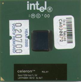
Figure 5: Celeron Coppermine with FC-PGA packaging.
Main features of Celeron Coppermine were:
- Based on Pentium III with Coppermine core
- Manufacturing process: 0.18 μm
- L1 cache: 32 KB total, 16 KB for instructions and 16 KB for data
- L2 cache: 128 KB
- External clock rate: 66 MHz (models up to 766 MHz) or 100 MHz (models starting at 800 MHz)
- Packaging: FC-PGA
- Socket: Socket 370
- Added support to SSE instructions
Available models of Celeron Coppermine are listed on the chart below. TDP stands for Thermal Design Power and indicates the CPU maximum thermal dissipation.
| Modelo | Internal Clock | External Clock | Voltage | TDP |
| SL46S | 533 MHz | 66 MHz | 1.5 V | 11.2 W |
| SL3W7 | 566 MHz | 66 MHz | 1.5 V | 11.9 W |
| SL4PC | 566 MHz | 66 MHz | 1.7 V | 11.9 W |
| SL4NW | 566 MHz | 66 MHz | 1.7 V | 11.9 W |
| SL46T | 566 MHz | 66 MHz | 1.5 V | 11.9 W |
| SL3W8 | 600 MHz | 66 MHz | 1.5 V | 12.6 W |
| SL46U | 600 MHz | 66 MHz | 1.5 V | 12.6 W |
| SL4PB | 600 MHz | 66 MHz | 1.7 V | 12.6 W |
| SL4NX | 600 MHz | 66 MHz | 1.7 V | 12.6 W |
| SL3VS | 633 MHz | 66 MHz | 1.65 V | 16.5 W |
| SL4PA | 633 MHz | 66 MHz | 1.7 V | 16.5 W |
| SL3W9 | 633 MHz | 66 MHz | 1.6 V | 16.5 W |
| SL4NY | 633 MHz | 66 MHz | 1.7 V | 16.5 W |
| SL4AB | 667 MHz | 66 MHz | 1.65 V | 17.5 W |
| SL4NZ | 667 MHz | 66 MHz | 1.7 V | 17.5 W |
| SL48E | 667 MHz | 66 MHz | 1.65 V | 17.5 W |
| SL4P9 | 667 MHz | 66 MHz | 1.7 V | 17.5 W |
| SL48F | 700 MHz | 66 MHz | 1.65 V | 18.3 W |
| SL4P2 | 700 MHz | 66 MHz | 1.7 V | 18.3 W |
| SL4P8 | 700 MHz | 66 MHz | 1.75 V | 18.3 W |
| SL4E6 | 700 MHz | 66 MHz | 1.6 V | 18.3 W |
| SL4P3 | 733 MHz | 66 MHz | 1.6 V | 19.1 W |
| SL4P7 | 733 MHz | 66 MHz | 1.7 V | 19.1 W |
| SL52Y | 733 MHz | 66 MHz | 1.25 V – 1.4 V | 22.8 W |
| SL4QF | 766 MHz | 66 MHz | 1.6 V | 20 W |
| SL5EA | 766 MHz | 66 MHz | 1.75 V | 23.6 W |
| SL52X | 766 MHz | 66 MHz | 1.75 V | 23.6 W |
| SL4P6 | 766 MHz | 66 MHz | 1.7 V | 20 W |
| SL54P | 800 MHz | 100 MHz | 1.75 V | 24.5 W |
| SL5WW | 800 MHz | 100 MHz | 1.75 V | 24.5 W |
| SL55R | 800 MHz | 100 MHz | 1.7 V | 20.8 W |
| SL4TF | 800 MHz | 100 MHz | 1.7 V | 20.8 W |
| SL5EB | 800 MHz | 100 MHz | 1.75 V | 24.5 W |
| SL5WC | 800 MHz | 100 MHz | 1.75 V | 24.5 W |
| SL5GA | 850 MHz | 100 MHz | 1.7 V | 22.5 W |
| SL5GB | 850 MHz | 100 MHz | 1.7 V | 22.5 W |
| SL5WX | 850 MHz | 100 MHz | 1.75 V | 25.7 W |
| SL54Q | 850 MHz | 100 MHz | 1.25 V – 1.4 V | 25.7 W |
| SL5EC | 850 MHz | 100 MHz | 1.75 V | 25.7 W |
| SL5WB | 850 MHz | 100 MHz | 1.75 V | 25.7 W |
| SL633 | 900 MHz | 100 MHz | 1.75 V | 30 W |
| SL5WY | 900 MHz | 100 MHz | 1.75 V | 26.7 W |
| SL5LX | 900 MHz | 100 MHz | 1.75 V | 26.7 W |
| SL5WA | 900 MHz | 100 MHz | 1.75 V | 26.7 W |
| SL5MQ | 900 MHz | 100 MHz | 1.75 V | 26.7 W |
| SL5UZ | 950 MHz | 100 MHz | 1.75 V | 26.7 W |
| SL5V2 | 950 MHz | 100 MHz | 1.75 V | 26.7 W |
| SL634 | 950 MHz | 100 MHz | 1.75 V | 32 W |
| SL5XQ | 1GHz | 100 MHz | 1.75 V | 29 W |
| SL635 | 1GHz | 100 MHz | 1.75 V | 29 W |
| SL5XT | 1GHz | 100 MHz | 1.75 V | 29 W |
| SL5XU | 1.1GHz | 100 MHz | 1.75 V | 33 W |
| SL5XR | 1.1GHz | 100 MHz | 1.75 V | 33 W |
Celeron Tualatin was based on Pentium III Tualatin core and had no more than 44 million transistors. This increase on the number of transistors is due to the architecture technology used on Celeron Tualatin, which was of 0.13 µm (Celeron III used a 0.25 µm technology). There was an increase on L2 cache, which had 256 KB in this version.
Intel made Celeron Tualatin available for socket 370 on versions ranging from 900 MHz to 1.4 GHz. All these versions of Celeron Tualatin work externally at 100 MHz.
Celeron Tualatin used a new kind of chip package called FC-PGA2, which is different from FC-PGA because of its metallic plate on top of the processor. This metallic plate allows a better heat transference between the processor and the heatsink. This metallic plate also protects the processor core from possible damages that could happen during the cooler installation.
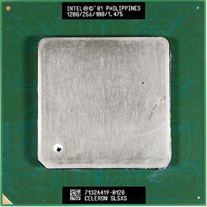
Figure 6: Celeron Tualatin with FC-PGA2 packaging.
In spite of the fact that Celeron Tualatin is a socket 370 processor, it cannot be installed on an old socket 370 motherboard. This is because Tualatin core redefined some 370 socket pins, which makes Celeron Tualatin incompatible for old motherboards. Thus, before buying a motherboard for your Celeron Tualatin, be sure that it is compatible with Tualatin core.
Main features of Celeron Tualatin were:
- Based on Pentium III with Tualatin core
- Manufacturing process: 0.13 μm
- L1 cache: 32 KB total, 16 KB for instructions and 16 KB for data
- L2 cache: 256 KB
- External clock rate: 100 MHz
- Packaging: FC-PGA2
- Socket: Socket 370
- SSE instructions
Available models of Celeron Tualatin are listed on the chart below. TDP stands for Thermal Design Power and indicates the CPU maximum thermal dissipation.
| Model | Internal Clock | Voltage | TDP |
| SL6JQ | 1 GHz | 1.5 V | 29.5 W |
| SL6CB | 1 GHz | 1.5 V | 29.5 W |
| SL5VP | 1 GHz | 1.5 V | 27.8 W |
| SL5ZF | 1 GHz | 1.5 V | 27.8 W |
| SL5ZE | 1.1 GHz | 1.5 V | 28.9 W |
| SL6RM | 1.1 GHz | 1.5 V | 28.9 W |
| SL6JR | 1.1 GHz | 1.5 V | 29.5 W |
| SL5VQ | 1.1 GHz | 1.5 V | 28.9 W |
| SL6CA | 1.1 GHz | 1.5 V | 30.8 W |
| SL656 | 1.2 GHz | 1.5 V | 32.1 W |
| SL6RP | 1.2 GHz | 1.5 V | 29.9 W |
| SL5Y5 | 1.2 GHz | 1.5 V | 29.9 W |
| SL6JS | 1.2 GHz | 1.5 V | 32 W |
| SL5XS | 1.2 GHz | 1.5 V | 29.9 W |
| SL68P | 1.2 GHz | 1.5 V | 32 W |
| SL6C8 | 1.2 GHz | 1.5 V | 32 W |
| SL6JT | 1.3 GHz | 1.5 V | 32 W |
| SL5ZJ | 1.3 GHz | 1.5 V | 33.4 W |
| SL6C7 | 1.3 GHz | 1.5 V | 32 W |
| SL5VR | 1.3 GHz | 1.5 V | 33.4 W |
| SL64V | 1.4 GHz | 1.5 V | 34.8 W |
| SL68G | 1.4 GHz | 1.5 V | 34.8 W |
| SL6JV | 1.4 GHz | 1.5 V | 33.2 W |
| SL6JU | 1.4 GHz | 1.5 V | – |
| SL6C6 | 1.4 GHz | 1.5 V | – |
Celeron Willamette is a 7th generation processor based on Pentium 4 Willamette core. It uses the FC-PGA2 packaging and is installed on socket 478 motherboards. It is important to remember that the first Pentium 4 models used socket 423 motherboards and no version of Celeron was launched for this kind of socket.
The architecture of Celeron Willamette L1 cache is completely different from other Celeron models presented until now, being based on the same architecture used by Pentium 4 processor. Instead of having a L1 data cache and a L1 instruction cache, this Celeron version has a 8KB L1 data cache and a trace execution cache.
The trace execution cache is located between the instruction decoder and the execution unit and is used to store the instructions already decoded. This cache stores up to 12 K microinstructions. Since each microinstruction has approximately 100 bits, this cache unit stores around 150 KB of data.
Another difference between this Celeron model and the previous ones is that it uses a 256-bit data path to communicate with its L2 memory cache, while this communication was previously done using a 64-bit or 128-bit data path.
Another important detail regarding Celeron Willamette is about its external bus operation. Celeron Willamette transfers not only one, but four data per clock pulse. So, the performance of its external bus is four times higher than a conventional external bus which runs with the same clock. Celeron Willamette works externally at a speed of 400 MHz (100 MHz x 4) reaching a theoretical maximum transfer rate of 3.2 GB/s.
Celeron Willamette was built using a process of 0.18 µm. It gives support to SSE2, and is available on versions ranging from 1.7 GHz to 1.8 GHz.
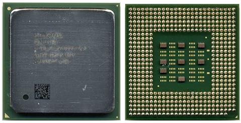
Figure 7: Celeron Willamette with FC-PGA2 packaging.
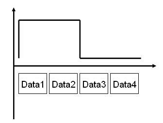
Figure 8: Celeron Willamette external bus works transferring four data for each clock pulse.
The only difference between Celeron Willamette and Northwood resides in the fact that Celeron Northwood is based on Pentium 4 Northwood core and was built with a technology of 0.13 µm. Everything said about Celeron Willamette is also valid for Celeron Northwood, which is available in clocks ranging from 2.0 GHz to 2.8 GHz.
Main features of Celeron Willamette and Northwood were:
- Based on Pentium 4 with Willamette core (models up to 1.8 GHz) or Northwood core (models starting at 2 GHz)
- Manufacturing process: 0.18 μm (for models based on Willamette core) or 13 μm (for models based on Northwood core)
- L1 cache: 8 KB for data and 150 KB trace cache
- L2 cache: 128 KB
- External clock rate: 400 MHz (100 MHz transferring four data per clock cycle)
- Packaging: FC-PGA2
- Socket: Socket 478
- Added support to SSE2 instructions, keeping support to SSE
Available models of Celeron Willamette and Northwood are listed on the chart below. TDP stands for Thermal Design Power and indicates the CPU maximum thermal dissipation.
| Model | Internal Clock | Voltage | TDP | Technology |
| SL68C | 1.7 GHz | 1.75 V | 63.5 W | 0.18 µm |
| SL69Z | 1.7 GHz | 1.75 V | 63.5 W | 0.18 µm |
| SL6A2 | 1.8 GHz | 1.75 V | 66.1 W | 0.18 µm |
| SL7RU | 1.8 GHz | 1.475 V – 1.525 V | 59.1 W | 0.18 µm |
| SL68D | 1.8 GHz | 1.75 V | 66.1 W | 0.18 µm |
| SL6LC | 2 GHz | 1.53 V | 52.8 W | 0.13 µm |
| SL68F | 2 GHz | 1.75 V | – | 0.13 µm |
| SL6HY | 2 GHz | 1.53 V | 52.8 W | 0.13 µm |
| SL6RV | 2 GHz | 1.25 V – 1.525 V | 52.8 W | 0.13 µm |
| SL6VY | 2 GHz | 1.25 V – 1.525 V | 52.8 W | 0.13 µm |
| SL6SW | 2 GHz | 1.525 V | 52.8 W | 0.13 µm |
| SL6VR | 2 GHz | 1.25 V – 1.525 V | 52.8 W | 0.13 µm |
| SL6SY | 2.1 GHz | 1.525 V | 55.5 W | 0.13 µm |
| SL6RS | 2.1 GHz | 1.25 V – 1.525 V | 55.5 W | 0.13 µm |
| SL6VZ | 2.1 GHz | 1.25 V – 1.525 V | 55.5 W | 0.13 µm |
| SL6VS | 2.1 GHz | 1.25 V – 1.525 V | 55.5 W | 0.13 µm |
| SL6SX | 2.2 GHz | 1.525 V | 57.1 W | 0.13 µm |
| SL6W2 | 2.2 GHz | 1.25 V – 1.525 V | 57.1 W | 0.13 µm |
| SL6VT | 2.2 GHz | 1.25 V – 1.525 V | 57.1 W | 0.13 µm |
| SL6RW | 2.2 GHz | 1.25 V – 1.525 V | 57.1 W | 0.13 µm |
| SL6T2 | 2.3 GHz | 1.5 V | 58.3 W | 0.13 µm |
| SL6XJ | 2.3 GHz | 1.25 V – 1.525 V | 58.3 W | 0.13 µm |
| SL6T3 | 2.3 GHz | 1.525 V | 58.3 W | 0.13 µm |
| SL6T5 | 2.3 GHz | 1.525 V | 58.3 W | 0.13 µm |
| SL6WD | 2.3 GHz | 1.25 V – 1.525 V | 58.3 W | 0.13 µm |
| SL6VU | 2.4 GHz | 1.25 V – 1.525 V | 59.8 W | 0.13 µm |
| SL6W4 | 2.4 GHz | 1.25 V – 1.525 V | 59.8 W | 0.13 µm |
| SL6XG | 2.4 GHz | 1.525 V | 59.8 W | 0.13 µm |
| SL72B | 2.5 GHz | 1.25 V – 1.525 V | 61 W | 0.13 µm |
| SL6ZY | 2.5 GHz | 1.25 V – 1.525 V | 61 W | 0.13 µm |
| SL6W5 | 2.6 GHz | 1.25 V – 1.525 V | 62.6 W | 0.13 µm |
| SL6VV | 2.6 GHz | 1.25 V – 1.525 V | 62.6 W | 0.13 µm |
| SL77S | 2.7 GHz | 1.25 V – 1.525 V | 66.8 W | 0.13 µm |
| SL77U | 2.7 GHz | 1.25 V – 1.525 V | 66.8 W | 0.13 µm |
| SL77V | 2.8 GHz | 1.25 V – 1.525 V | 68.4 W | 0.13 µm |
| SL77T | 2.8 GHz | 1.25 V – 1.525 V | 68.4 W | 0.13 µm |
Celeron D is based on Pentium 4 Prescott core and is built on 90- or 65-nanometer technology.
Celeron D has a L1 data cache of 16 KB, a L2 memory cache of 256 KB, works externally at 533 MHz (133 MHz transferring four data per each clock cycle), gives support to the multimedia instructions SSE3, FC-PGA2 packaging, socket 478 or 775 and can be found with c
lock speed ranging from 2.53 GHz to 3.2 GHz. Being a simplified version of Pentium 4 Prescott, Celeron D does not support the Hyper-Threading technology, which allows the simulation of two logical processors on one single material processor that is present on Pentium 4 processors.
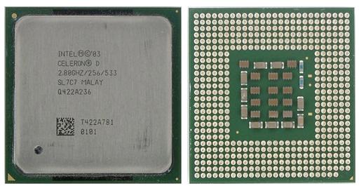
Figure 9: 2.8 GHz Celeron D with socket 478 pin.
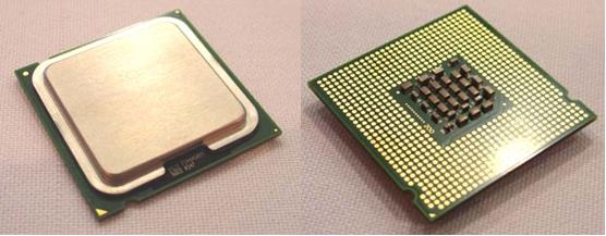
Figure 10: 775 pin layout used by Pentium 4 and Celeron D processors.
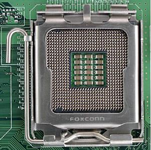
Figure 11: Detail of a 775 socket. Note that the pins are situated on the socket and not on the processor.
Main features of Celeron D are:
- Based on Pentium 4 with Prescott core
- Manufacturing process: 90 nm or 65 nm
- L1 cache: 16 KB for data and 150 KB trace cache
- L2 cache: 256 KB
- External clock rate: 533 MHz (133 MHz transferring four data per clock cycle)
- Packaging: FC-PGA2 (socket 478) or FC-LGA (socket LGA775)
- Socket: Socket 478 or Socket LGA775
- Added support to SSE3 instructions, keeping support to SSE and SSE2
- Execute Disable technology on selected models
- EM64T Technology (a.k.a. “64-bit technology”) on selected models
Available models of Celeron D are listed on the chart below. TDP stands for Thermal Design Power and indicates the CPU maximum thermal dissipation.
| sSpec | Model | Internal Clock | L2 Cache | Voltage | TDP |
| SL9KJ | 365 | 3.60 GHz | 512 KB | 1.25 V – 1.30 V | 65 W |
| SL9KK | 360 | 3.46 GHz | 512 KB | 1.25 V – 1.30 V | 65 W |
| SL96N | 356 | 3.33 GHz | 512 KB | 1.25 V – 1.30 V | 86 W |
| SL8HS | 355 | 3.33 GHz | 256 KB | 1.25 V – 1.40 V | 73 W |
| SL8HF | 351 | 3.20 GHz | 256 KB | 1.25 V – 1.40 V | 84 W |
| SL96P | 352 | 3.20 GHz | 512 KB | 1.25 V – 1.30 V | 86 W |
| SL8HQ | 350 | 3.20 GHz | 256 KB | 1.25 V – 1.40 V | 73 W |
| SL9BS | 351 | 3.20 GHz | 256 KB | 1.25 V – 1.40 V | 73 W |
| SL7TZ | 351 | 3.20 GHz | 256 KB | 1.25 V – 1.40 V | 84 W |
| SL7NY | N/A | 3.20 GHz | 256 KB | 1.25 V – 1.40 V | 73 W |
| SL8HP | 345 | 3.06 GHz | 256 KB | 1.25 V – 1.40 V | 73 W |
| SL7W3 | 345 | 3.06 GHz | 256 KB | 1.25 V – 1.40 V | 73 W |
| SL7VV | 345J | 3.06 GHz | 256 KB | 1.25 V – 1.40 V | 84 W |
| SL7TY | 346 | 3.06 GHz | 256 KB | 1.25 V – 1.40 V | 84 W |
| SL8HD | 346 | 3.06 GHz | 256 KB | 1.25 V – 1.40 V | 84 W |
| SL7TQ | 345J | 3.06 GHz | 256 KB | 1.25 V – 1.40 V | 84 W |
| SL9KN | 347 | 3.06 GHz | 512 KB | 1.25 V – 1.40 V | 65 W |
| SL9BR | 346 | 3.06 GHz | 256 KB | 1.25 V – 1.40 V | 84 W |
| SL7DN | 345 | 3.06 GHz | 256 KB | 1.25 V – 1.40 V | 73 W |
| SL7NX | 345 | 3.06 GHz | 256 KB | 1.25 V – 1.40 V | 73 W |
| SL9XU | 347 | 3.06 GHz | 512 KB | 1.25 V – 1.40 V | 86 W |
| SL7TP | 340J | 2.93 GHz | 256 KB | 1.25 V – 1.40 V | 84 W |
| SL8HB | 341 | 2.93 GHz | 256 KB | 1.25 V – 1.40 V | 84 W |
| SL7W2 | 340 | 2.93 GHz | 256 KB | 1.25 V – 1.40 V | 73 W |
| SL7TX | 341 | 2.93 GHz | 256 KB | 1.25 V – 1.40 V | 84 W |
| SL7TS | 340 | 2.93 GHz | 256 KB | 1.25 V – 1.40 V | 73 W |
| SL7RN | 340 | 2.93 GHz | 256 KB | 1.287 V – 1.40 V | 73 W |
| SL7SV | 340 | 2.93 GHz | 256 KB | 1.25 V – 1.40 V | 84 W |
| SL8HN | 340 | 2.93 GHz | 256 KB | 1.25 V – 1.40 V | 73 W |
| SL7Q9 | 340 | 2.93 GHz | 256 KB | 1.25 V – 1.40 V | 73 W |
| SL7C7 | 335 | 2.80 GHz | 256 KB | 1.25 V – 1.40 V | 73 W |
| SL7NW | 335 | 2.80 GHz | 256 KB | 1.25 V – 1.40 V | 73 W |
| SL7VT | 335J | 2.80 GHz | 256 KB | 1.25 V – 1.40 V | 84 W |
| SL7TJ | 335 | 2.80 GHz | 256 KB | 1.25 V – 1.40 V | 73 W |
| SL7TN | 335J | 2.80 GHz | 256 KB | 1.287 V – 1.40 V | 84 W |
| SL7L2 | 335 | 2.80 GHz | 256 KB | 1.287 V – 1.40 V | 73 W |
| SL7SU | 335 | 2.80 GHz | 256 KB | 1.25 V – 1.40 V | 84 W |
| SL7TW | 336 | 2.80 GHz | 256 KB | 1.25 V – 1.40 V | 84 W |
| SL7DM | 335 | 2.80 GHz | 256 KB | 1.25 V – 1.40 V | 73 W |
| SL98W | 336 | 2.80 GHz | 256 KB | 1.25 V – 1.40 V | 84 W |
| SL7VZ | 335 | 2.80 GHz | 256 KB | 1.25 V – 1.40 V | 73 W |
| SL8HM | 335 | 2.80 GHz | 256 KB | 1.25 V – 1.40 V | 73 W |
| SL8H9 | 336 | 2.80 GHz | 256 KB | 1.25 V – 1.40 V | 84 W |
| SL7TV | 331 | 2.66 GHz | 256 KB | 1.25 V – 1.40 V | 84 W |
| SL7NV | 330 | 2.66 GHz | 256 KB | 1.287 V – 1.40 V | 73 W |
| SL8H7 | 331 | 2.66 GHz | 256 KB | 1.25 V – 1.40 V | 84 W |
| SL7TH | 330 | 2.66 GHz | 256 KB | 1.25 V – 1.40 V | 73 W |
| SL8HL | 330 | 2.66 GHz | 256 KB | 1.25 V – 1.40 V | 73 W |
| SL7TM | 330J | 2.66 GHz | 256 KB | 1.287 V – 1.40 V | 84 W |
| SL7ST | 330 | 2.66 GHz | 256 KB | 1.25 V – 1.40 V | 84 W |
| SL98V | 331 | 2.66 GHz | 256 KB | 1.25 V – 1.40 V | 84 W |
| SL7DL | 330 | 2.66 GHz | 256 KB | 1.25 V – 1.40 V | 73 W |
| SL7VS | 330J | 2.66 GHz | 256 KB | 1.25 V – 1.40 V | 84 W |
| SL7C6 | 330 | 2.66 GHz | 256 KB | 1.25 V – 1.40 V | 73 W |
| SL7KZ | 330 | 2.66 GHz | 256 KB | 1.25 V – 1.40 V | 73 W |
| SL7VY | 330 | 2.66 GHz | 256 KB | 1.25 V – 1.40 V | 73 W |
| SL7SS | 325 | 2.53 GHz | 256 KB | 1.25 V – 1.40 V | 84 W |
| SL7C5 | 325 | 2.53 GHz | 256 KB | 1.25 V – 1.40 V | 73 W |
| SL7NU | 325 | 2.53 GHz | 256 KB | 1.25 V – 1.40 V | 73 W |
| SL7ND | 325 | 2.53 GHz | 256 KB | 1.287 V – 1.40 V | 73 W |
| SL98U | 326 | 2.53 GHz | 256 KB | 1.25 V – 1.40 V | 84 W |
| SL7KY | 325 | 2.53 GHz | 256 KB | 1.287 V – 1.40 V | 73 W |
| SL8HK | 325 | 2.53 GHz | 256 KB | 1.25 V – 1.40 V | 73 W |
| SL7VR | 325J | 2.53 GHz | 256 KB | 1.25 V – 1.40 V | 84 W |
| SL8H5 | 326 | 2.53 GHz | 256 KB | 1.25 V – 1.40 V | 84 W |
| SL7TU | 326 | 2.53 GHz | 256 KB | 1.25 V – 1.40 V | 84 W |
| SL7VX | 325 | 2.53 GHz | 256 KB | 1.25 V – 1.40 V | 73 W |
| SL7TL | 325J | 2.53 GHz | 256 KB | 1.287 V – 1.40 V | 84 W |
| SL7TG | 325 | 2.53 GHz | 256 KB | 1.25 V – 1.40 V | 73 W |
| SL7C4 | 320 | 2.40 GHz | 256 KB | 1.25 V – 1.40 V | 73 W |
| SL7KX | 320 | 2.40 GHz | 256 KB | 1.25 V – 1.40 V | 73 W |
| SL7VW | 320 | 2.40 GHz | 256 KB | 1.287 V – 1.40 V | 73 W |
| SL7VQ | 320 | 2.40 GHz | 256 KB | 1.25 V – 1.40 V | 84 W |
| SL7JV | 320 | 2.40 GHz | 256 KB | 1.25 V – 1.40 V | 73 W |
| SL8HJ | 320 | 2.40 GHz | 256 KB | 1.25 V – 1.40 V | 73 W |
| SL7XG | 315 | 2.26 GHz | 256 KB | 1.287 V – 1.40 V | 73 W |
| SL8HH | 315 | 2.26 GHz | 256 KB | 1.25 V – 1.40 V | 73 W |
| SL7WS | 315 | 2.26 GHz | 256 KB | 1.25 V – 1.40 V | 73 W |
| SL93Q | 315 | 2.26 GHz | 256 KB | 1.25 V – 1.40 V | 73 W |
| SL87K | 315 | 2.26 GHz | 256 KB | 1.287 V – 1.40 V | 73 W |
| SL7XY | N/A | 2.26 GHz | 256 KB | 1.287 V – 1.40 V | 73 W |
| SL8AW | 315 | 2.26 GHz | 256 KB | 1.25 V – 1.40 V | 73 W |
| SL8RZ | 310 | 2.13 GHz | 256 KB | 1.25 V – 1.40 V | 73 W |
| SL93R | 310 | 2.13 GHz | 256 KB | 1.25 V – 1.40 V | 73 W |
| SL8S4 | 310 | 2.13 GHz | 256 KB | 1.25 V – 1.40 V | 73 W |
| SL8S2 | 310 | 2.13 GHz | 256 KB | 1.25 V – 1.40 V | 73 W |
| sSpec | Model | Technology | Socket | Execute Disable | EM64T |
| SL9KJ | 365 | 65 nm | 775 | Yes | Yes |
| SL9KK | 360 | 65 nm | 775 | Yes | Yes |
| SL96N | 356 | 65 nm | 775 | Yes | Yes |
| SL8HS | 355 | 90 nm | 775 | Yes | Yes |
| SL8HF | 351 | 90 nm | 775 | Yes | Yes |
| SL96P | 352 | 65 nm | 775 | Yes | Yes |
| SL8HQ | 350 | 90 nm | 478 | No | No |
| SL9BS | 351 | 90 nm | 775 | Yes | Yes |
| SL7TZ | 351 | 90 nm | 775 | Yes | Yes |
| SL7NY | N/A | 90 nm | 478 | No | No |
| SL8HP | 345 | 90 nm | 478 | No | No |
| SL7W3 | 345 | 90 nm | 478 | No | No |
| SL7VV | 345J | 90 nm | 775 | Yes | No |
| SL7TY | 346 | 90 nm | 775 | Yes | Yes |
| SL8HD | 346 | 90 nm | 775 | Yes | Yes |
| SL7TQ | 345J | 90 nm | 775 | Yes | No |
| SL9KN | 347 | 65 nm | 775 | Yes | Yes |
| SL9BR | 346 | 90 nm | 775 | No | Yes |
| SL7DN | 345 | 90 nm | 478 | No | No |
| SL7NX | 345 | 90 nm | 478 | No | No |
| SL9XU | 347 | 65 nm | 775 | No | Yes |
| SL7TP | 340J | 90 nm | 775 | No | No |
| SL8HB | 341 | 90 nm | 775 | No | Yes |
| SL7W2 | 340 | 90 nm | 478 | No | No |
| SL7TX | 341 | 90 nm | 775 | No | Yes |
| SL7TS | 340 | 90 nm | 478 | No | No |
| SL7RN | 340 | 90 nm | 478 | No | No |
| SL7SV | 340 | 90 nm | 775 | No | No |
| SL8HN | 340 | 90 nm | 478 | No | No |
| SL7Q9 | 340 | 90 nm | 478 | No | No |
| SL7C7 | 335 | 90 nm | 478 | No | No |
| SL7NW | 335 | 90 nm | 478 | No | No |
| SL7VT | 335J | 90 nm | 775 | Yes | No |
| SL7TJ | 335 | 90 nm | 478 | No | No |
| SL7TN | 335J | 90 nm | 775 | Yes | No |
| SL7L2 | 335 | 90 nm | 478 | No | No |
| SL7SU | 335 | 90 nm | 775 | No | No |
| SL7TW | 336 | 90 nm | 775 | Yes | Yes |
| SL7DM | 335 | 90 nm | 478 | No | No |
| SL98W | 336 | 90 nm | 775 | No | Yes |
| SL7VZ | 335 | 90 nm | 478 | No | No |
| SL8HM | 335 | 90 nm | 478 | No | No |
| SL8H9 | 336 | 90 nm | 775 | Yes | Yes |
| SL7TV | 331 | 90 nm | 775 | Yes | Yes |
| SL7NV | 330 | 90 nm | 478 | No | No |
| SL8H7 | 331 | 90 nm | 775 | No | Yes |
| SL7TH | 330 | 90 nm | 478 | No | No |
| SL8HL | 330 | 90 nm | 478 | No | No |
| SL7TM | 330J | 90 nm | 775 | Yes | No |
| SL7ST | 330 | 90 nm | 775 | No | No |
| SL98V | 331 | 90 nm | 775 | No | Yes |
| SL7DL | 330 | 90 nm | 478 | No | No |
| SL7VS | 330J | 90 nm | 775 | Yes | No |
| SL7C6 | 330 | 90 nm | 478 | No | No |
| SL7KZ | 330 | 90 nm | 478 | No | No |
| SL7VY | 330 | 90 nm | 478 | No | No |
| SL7SS | 325 | 90 nm | 775 | No | No |
| SL7C5 | 325 | 90 nm | 478 | No | No |
| SL7NU | 325 | 90 nm | 478 | No | No |
| SL7ND | 325 | 90 nm | 478 | No | No |
| SL98U | 326 | 90 nm | 775 | No | Yes |
| SL7KY | 325 | 90 nm | 478 | No | No |
| SL8HK | 325 | 90 nm | 478 | No | No |
| SL7VR | 325J | 90 nm | 775 | Yes | No |
| SL8H5 | 326 | 90 nm | 775 | Yes | Yes |
| SL7TU | 326 | 90 nm | 775 | Yes | Yes |
| SL7VX | 325 | 90 nm | 478 | No | No |
| SL7TL | 325J | 90 nm | 775 | Yes | No |
| SL7TG | 325 | 90 nm | 478 | No | No |
| SL7C4 | 320 | 90 nm | 478 | No | No |
| SL7KX | 320 | 90 nm | 478 | No | No |
| SL7VW | 320 | 90 nm | 478 | No | No |
| SL7VQ | 320 | 90 nm | 775 | Yes | No |
| SL7JV | 320 | 90 nm | 478 | No | No |
| SL8HJ | 320 | 90 nm | 478 | No | No |
| SL7XG | 315 | 90 nm | 478 | No | No |
| SL8HH | 315 | 90 nm | 478 | No | No |
| SL7WS | 315 | 90 nm | 478 | No | No |
| SL93Q | 315 | 90 nm | 478 | No | No |
| SL87K | 315 | 90 nm | 478 | No | No |
| SL7XY | N/A | 90 nm | 478 | No | No |
| SL8AW | 315 | 90 nm | 478 | No | No |
| SL8RZ | 310 | 90 nm | 478 | No | No |
| SL93R | 310 | 90 nm | 478 | No | No |
| SL8S4 | 310 | 90 nm | 478 | No | No |
| SL8S2 | 310 | 90 nm | 478 | No | No |
Celeron 400 series processors are based on Core microarchitecture, the same used by Core 2 Duo CPUs having, however, only one processing core (Core 2 Duo processors have two processing cores). Celeron 400 series main technical specs are:
- Based on Conroe-L core, the same one used by Core 2 Duo but with just one processing core
- Manufacturing process: 65 nm
- L1 cache: 64 KB total, 32 KB for instructions and 32 KB for data.
- L2 cache: 512 KB.
- External clock rate: 800 MHz (200 MHz transferring four data per clock cycle)
- Packaging: FC-LGA6
- Socket: Socket LGA775.
- SSE, SSE2 and SSE3 instructions
- Execute Disable technology
- EM64T technology (a.k.a. 64-bit technology)
Available models of Celeron 400 series are listed on the chart below. TDP stands for Thermal Design Power and indicates the CPU maximum thermal dissipation.
| sSPEC | Model | Internal Clock | Voltage | TDP |
| SLAFZ | 450 | 2.2 GHz | 1.0 V – 1.3375V | 35 W |
| SL9XL | 440 | 2 GHz | 1.050V – 1.300V | 35 W |
| SL9XN | 430 | 1.80 GHz | 1.050V – 1.300V | 35 W |
| SL9XP | 420 | 1.60 GHz | 1.050V – 1.300V | 35 W |
Intel is finally bringing dual-core technology to the Celeron family. At first this could sound contradictory since the goal of Celeron processors is to be a low-cost CPU targeted to those users that can’t or don’t want to pay for a CPU with the latest technological features available. However dual-core technology can’t be considered “the latest technological feature” anymore and historically what Intel does is to push what was once a high-end feature to the mainstream CPUs and then, after a while, to the entry-level CPUs. Since today’s high-end CPUs are quad-core and Intel has been selling only dual-core CPUs for the mainstream market for quite a while, not more natural than start introducing dual-core CPUs to the entry-level market as well. As you can see on a near future we will only have CPUs with at least two cores available on the market.
Dual-core Celeron processors are based on Core microarchitecture, the same used by Core 2 Duo CPUs. These CPUs are also known by the codename Allendale.
Celeron E1000 series main features are:
- Core microarchitecture
- Dual-core technology
- Manufacturing process: 65 nm
- L1 cache: 64 KB total, 32 KB for instructions and 32 KB for data.
- L2 cache: 512 KB, shared by the two cores
- External clock rate: 800 MHz (200 MHz transferring four data per clock cycle)
- Packaging: FC-LGA6
- Socket: Socket LGA775.
- SSE, SSE2 and SSE3 instructions
- Execute Disable technology
- EM64T technology (a.k.a. 64-bit technology)
- Enhanced SpeedStep technology
Available models of Celeron E1000 series are listed on the chart below. TDP stands for Thermal Design Power and indicates the CPU maximum thermal dissipation.
| sSpec | Model | Internal Clock | External Clock |
| SLAQW | E1200 | 1.6 GHz | 800 MHz |
| SLAR2 | E1400 | 2.0 GHz | 800 MHz |
| SLAQZ | E1500 | 2.2 GHz | 800 MHz |
| SLAQY | E1600 | 2.4 GHz | 800 MHz |
| sSpec | Model | TDP | Max. Temp. (°C) | Voltage (V) |
| SLAQW | E1200 | 65 W | 73.3 | 0.85 – 1.5 |
| SLAR2 | E1400 | 65 W | 73.3 | 0.85 – 1.5 |
| SLAQZ | E1500 | 65 W | 73.3 | 0.85 – 1.5 |
| SLAQY | E1600 | 65 W | 73.3 | 0.85 – 1.5 |
E3000 Series Celeron processors have two processing cores and they are based in 45 nm core microarchiteture (Penryn Core).
Celeron E3000 series main features are:
- Core microarchitecture
- Dual-core technology
- Manufacturing process: 45 nm
- L1 cache: 64 KB total, 32 KB for instructions and 32 KB for data.
- L2 cache: 1 MB, shared by the two cores
- External clock rate: 800 MHz (200 MHz transferring four data per clock cycle)
- Packaging: FC-LGA6
- Socket: Socket LGA775.
- SSE, SSE2, SSE3 and SSE4.1 instructions
- Execute Disable technology
- EM64T technology (a.k.a. 64-bit technology)
- Enhanced SpeedStep technology
- Intel Virtualization Technology
Available models of Celeron E3000 series are listed on the chart below. TDP stands for Thermal Design Power and indicates the CPU maximum thermal dissipation.
| sSpec | Model | Internal Clock | External Clock |
| SLGTY | E3500 | 2.7 GHz | 800 MHz |
| SLGTZ | E3400 | 2.6 GHz | 800 MHz |
| SLGU4 | E3300 | 2.5 GHz | 800 MHz |
| SLGU5 | E3200 | 2.4 GHz | 800 MHz |
| sSpec | Model | TDP | Max. Temp. (°C) | Voltage (V) |
| SLGTY | E3500 | 65 W | 74.1 | 0.85 – 1.3635 |
| SLGTZ | E3400 | 65 W | 74.1 | 0.85 – 1.3625 |
| SLGU4 | E3300 | 65 W | 74.1 | 0.85 – 1.3625 |
| SLGU5 | E3200 | 65 W | 74.1 | 0.85 – 1.3625 |