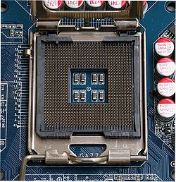
The second-generation Core i5 targeted to laptops, which use the Sandy Bridge microarchitecture, can use two different pinouts, BGA1023 or socket G2, and have an integrated dual-channel DDR3 memory controller supporting 1,066 MHz, 1,333 MHz, and 1,600 MHz DDR3 memories. They also have an integrated PCI Express 2.0 controller supporting one x16 connection, two x8 connections, one x8 connection or two x4 connections. Communication with the motherboard chipset is accomplished through a DMI bus (2 GB/s each direction, which is listed as 5 GT/s by Intel). These processors also have an integrated DirectX 10.1 video controller running at 350 MHz with a 1.2 GHz “boost” clock on models with a TDP of 17 W, or 650 MHz with a 1.3 GHz “boost” clock on models with a TDP of 35 W, all with 12 processing cores (HD 3000 graphics engine). All Core i5 mobile CPUs are dual-core processors supporting Hyper-Threading (HT) technology, which simulates two logical processing cores in each physical core. Therefore, they are recognized by the operating system as four-core CPUs.
sSpec
Model
Clock
Turbo Boost
SR0CS
2557M
1.7 GHz
2.7 GHz
SR044
2540M
2.6 GHz
3.3 GHz
SR046
2540M
2.6 GHz
3.3 GHz
SR03W
2537M
1.4 GHz
2.3 GHz
SR048
2520M
2.5 GHz
3.2 GHz
NA
2520M
2.5 GHz
3.2 GHz
SR02U
2510E
2.5 GHz
3.1 GHz
SR0D6
2467M
1.6 GHz
2.3 GHz
SR0CH
2450M
2.5 GHz
3.1 GHz
SR06Z
2450M
2.5 GHz
3.1 GHz
SR04Z
2450M
2.5 GHz
3.1 GHz
NA
2435M
2.4 GHz
3 GHz
NA
2435M
2.4 GHz
3 GHz
SR04W
2430M
2.4 GHz
3 GHz
NA
2430M
2.4 GHz
3 GHz
SR04B
2410M
2.3 GHz
2.9 GHz
SR04G
2410M
2.3 GHz
2.9 GHz
sSpec
Cores
HT
Video
SR0CS
2
Yes
HD 3000
SR044
2
Yes
HD 3000
SR046
2
Yes
HD 3000
SR03W
2
Yes
HD 3000
SR048
2
Yes
HD 3000
NA
2
Yes
HD 3000
SR02U
2
Yes
HD 3000
SR0D6
2
Yes
HD 3000
SR0CH
2
Yes
HD 3000
SR06Z
2
Yes
HD 3000
SR04Z
2
Yes
HD 3000
NA
2
Yes
HD 3000
NA
2
Yes
HD 3000
SR04W
2
Yes
HD 3000
NA
2
Yes
HD 3000
SR04B
2
Yes
HD 3000
SR04G
2
Yes
HD 3000
sSpec
Model
Video Clock
Video Boost
Tech.
SR0CS
2557M
350 MHz
1.2 GHz
32 nm
SR044
2540M
650 MHz
1.3 GHz
32 nm
SR046
2540M
650 MHz
1.3 GHz
32 nm
SR03W
2537M
350 MHz
1.2 GHz
32 nm
SR048
2520M
650 MHz
1.3 GHz
32 nm
NA
2520M
650 MHz
1.3 GHz
32 nm
SR02U
2510E
650 MHz
1.3 GHz
32 nm
SR0D6
2467M
350 MHz
1.2 GHz
32 nm
SR0CH
2450M
650 MHz
1.3 GHz
32 nm
SR06Z
2450M
650 MHz
1.3 GHz
32 nm
SR04Z
2450M
650 MHz
1.3 GHz
32 nm
NA
2435M
650 MHz
1.3 GHz
32 nm
NA
2435M
650 MHz
1.3 GHz
32 nm
SR04W
2430M
650 MHz
1.3 GHz
32 nm
NA
2430M
650 MHz
1.3 GHz
32 nm
SR04B
2410M
650 MHz
1.3 GHz
32 nm
SR04G
2410M
650 MHz
1.3 GHz
32 nm
sSpec
L3 Cache
TDP (W)
Max. Temp. (°C)*
Package
SR0CS
3 MiB
17
100
BGA1023
SR044
3 MiB
35
100
G2
SR046
3 MiB
35
100
BGA1023
SR03W
3 MiB
17
100
BGA1023
SR048
3 MiB
35
100
G2
NA
3 MiB
35
100
BGA1023
SR02U
3 MiB
35
100
G2
SR0D6
3 MiB
17
100
BGA1023
SR0CH
3 MiB
35
100
G2
SR06Z
3 MiB
35
100
BGA1023
SR04Z
3 MiB
35
100
BGA1023
NA
3 MiB
35
100
G2
NA
3 MiB
35
100
BGA1023
SR04W
3 MiB
35
100
G2
NA
3 MiB
35
100
BGA1023
SR04B
3 MiB
35
100
G2
SR04G
3 MiB
35
100
BGA1023
TDP stands for Thermal Design Power and indicates the CPU maximum thermal dissipation, i.e., the CPU cooler must be able to dissipate at least this amount of heat. * The temperatures listed above are Tjunction, which is the maximum internal temperature of the CPU. On some other models, the manufacturer lists Tcase, which is the maximum external temperature of the CPU. The two are not comparable.
The Core i5-3xxx models are based on the Ivy Bridge microarchitecture and are also known as the third-generation Core i5 processors. They use the socket LGA1155, the same used by the second-generation Core i5 processors. The integrated memory controller supports dual-channel architecture as well as 1,333 MHz and 1,600 MHz DDR3 memories. They have an integrated PCI Express 3.0 controller supporting one x16 connection, two x8 connections, one x8 connection or two x4 connections. Communication with the motherboard chipset is achieved through a DMI bus (2 GB/s each direction, which is listed as 5 GT/s by Intel). All models (except the “P” models) have an integrated DirectX 11 video controller with six (Intel HD 2500 graphics) or 12 (Intel HD 4000 graphics) processing units, running at 650 MHz with a “boost” clock of 1.25 GHz on 35xx models, 1.1 GHz on 34xx models or 1.05 GHz on 33xx models. Models with integrated video support three displays (previous generations support two).
sSpec
Model
Clock
Turbo Boost
SR0PM
3570K
3.4 GHz
3.8 GHz
SR0T7
3570
3.4 GHz
3.8 GHz
SR0P1
3570T
2.3 GHz
3.3 GHz
SR0T9
3570S
3.1 GHz
3.8 GHz
SR0P0
3550
3.3 GHz
3.7 GHz
SR0P3
3550S
3 GHz
3.7 GHz
SR0PP
3475S
2.9 GHz
3.6 GHz
SR0T8
3470
3.2 GHz
3.6 GHz
SR0RJ
3470T
2.9 GHz
3.6 GHz
SR0TA
3470S
2.9 GHz
3.6 GHz
SR0PF
3450
3.1 GHz
3.5 GHz
SR0P2
3450S
2.8 GHz
3.5 GHz
SR0WS
3350P
3.1 GHz
3.3 GHz
SR0RQ
3330
3 GHz
3.2 GHz
SR0RR
3330S
2.7 GHz
3.2 GHz
sSpec
Cores
HT
Video
SR0PM
4
No
HD 4000
SR0T7
4
No
HD 2500
SR0P1
4
No
HD 2500
SR0T9
4
No
HD 2500
SR0P0
4
No
HD 2500
SR0P3
4
No
HD 2500
SR0PP
4
No
HD 2500
SR0T8
4
No
HD 2500
SR0RJ
4
No
HD 2500
SR0TA
4
No
HD 2500
SR0PF
4
No
HD 2500
SR0P2
4
No
HD 2500
SR0WS
4
No
No
SR0RQ
4
No
HD 2500
SR0RR
4
No
HD 2500
sSpec
Model
Video Clock
Video Boost
Tech.
SR0PM
3570K
650 MHz
1.15 GHz
22 nm
SR0T7
3570
650 MHz
1.15 GHz
22 nm
SR0P1
3570T
650 MHz
1.15 GHz
22 nm
SR0T9
3570S
650 MHz
1.15 GHz
22 nm
SR0P0
3550
650 MHz
1.15 GHz
22 nm
SR0P3
3550S
650 MHz
1.1 GHz
22 nm
SR0PP
3475S
650 MHz
1.1 GHz
22 nm
SR0T8
3470
650 MHz
1.1 GHz
22 nm
SR0RJ
3470T
650 MHz
1.1 GHz
22 nm
SR0TA
3470S
650 MHz
1.1 GHz
22 nm
SR0PF
3450
650 MHz
1.1 GHz
22 nm
SR0P2
3450S
650 MHz
1.1 GHz
22 nm
SR0WS
3350P
No
1.05 GHz
22 nm
SR0RQ
3330
650 MHz
1.05 GHz
22 nm
SR0RR
3330S
650 MHz
1.05 GHz
22 nm
sSpec
L3 Cache
TDP (W)
Max. Temp. (°C)*
Voltage (V)
SR0PM
6 MiB
77
67.4
NA
SR0T7
6 MiB
77
67.4
NA
SR0P1
6 MiB
45
69.8
NA
SR0T9
6 MiB
65
69.1
NA
SR0P0
6 MiB
77
67.4
NA
SR0P3
6 MiB
65
69.1
NA
SR0PP
6 MiB
65
69.1
NA
SR0T8
6 MiB
77
67.4
NA
SR0RJ
6 MiB
35
65.0
NA
SR0TA
6 MiB
65
69.1
NA
SR0PF
6 MiB
77
67.4
NA
SR0P2
6 MiB
65
69.1
NA
SR0WS
6 MiB
69
67.4
NA
SR0RQ
6 MiB
77
67.4
NA
SR0RR
6 MiB
65
NA
NA
TDP stands for Thermal Design Power and indicates the CPU maximum thermal dissipation, i.e., the CPU cooler must be able to dissipate at least this amount of heat. * The temperatures listed above are Tcase, which is the maximum external temperature of the CPU. On some other models, the manufacturer lists Tjunction, which is the maximum internal temperature of the CPU. The two are not comparable.
As their desktop counterparts, the Core i5-3xxx models targeted to mobile computers are based on the Ivy Bridge microarchitecture and are also known as the third-generation Core i5 processors. They can use either the BGA1023 pinout or the socket S2 pinout. The integrated memory controller supports dual-channel architecture as well as 1,333 MHz and 1,600 MHz DDR3, DDR3L, and DDR3L-RS memories. They also have an integrated PCI Express 3.0 controller supporting one x16 connection, two x8 connections, one x8 connection or two x4 connections. Communication with the motherboard chipset is accomplished through a DMI bus (2 GB/s each direction, which is listed as 5 GT/s by Intel). All models have an integrated DirectX 11 video controller with 12 execution units (Intel HD 4000 graphics). This is one of the main differences between the mobile and the desktop models, since desktop models use the Intel HD 2500 graphics (six execution units). On “M” models, the graphics engine works at 650 MHz with 1.2 GHz at “boost” mode, while on “U” models, the graphics engine works at 350 MHz with a “boost” mode of 1.15 GHz on 34xx models or 1.05 GHz on 33xx models. All models support three displays (previous generations support two). Differently from the desktop models, mobile third-generation Core i5 processors are dual-core CPUs with Hyper-Threading (HT) technology, which simulates two logical processing cores in each physical core. Therefore, they are recognized by the operating system as four-core CPUs.
sSpec
Model
Clock
Turbo Boost
SR0N7
3427U
1.8 GHz
2.8 GHz
SR0MV
3360M
2.8 GHz
3.5 GHz
SR0MW
3360M
2.8 GHz
3.5 GHz
SR0MX
3320M
2.6 GHz
3.3 GHz
SR0MY
3320M
2.6 GHz
3.3 GHz
SR0N8
3317U
1.7 GHz
2.6 GHz
SR0MZ
3210M
2.5 GHz
3.1 GHz
NA
3210M
2.5 GHz
3.1 GHz
sSpec
Cores
HT
Video
SR0N7
2
Yes
HD 4000
SR0MV
2
Yes
HD 4000
SR0MW
2
Yes
HD 4000
SR0MX
2
Yes
HD 4000
SR0MY
2
Yes
HD 4000
SR0N8
2
Yes
HD 4000
SR0MZ
2
Yes
HD 4000
NA
2
Yes
HD 4000
sSpec
Model
Video Clock
Video Boost
Tech.
SR0N7
3427U
350 MHz
1.15 GHz
22 nm
SR0MV
3360M
650 MHz
1.2 GHz
22 nm
SR0MW
3360M
650 MHz
1.2 GHz
22 nm
SR0MX
3320M
650 MHz
1.2 GHz
22 nm
SR0MY
3320M
650 MHz
1.2 GHz
22 nm
SR0N8
3317U
350 MHz
1.05 GHz
22 nm
SR0MZ
3210M
650 MHz
1.2 GHz
22 nm
NA
3210M
650 MHz
1.2 GHz
22 nm
sSpec
L3 Cache
TDP (W)
Max. Temp. (°C)*
Package
SR0N7
3 MiB
17
105
BGA1023
SR0MV
3 MiB
35
105
G2
SR0MW
3 MiB
35
105
BGA1023
SR0MX
3 MiB
35
105
G2
SR0MY
3 MiB
35
105
BGA1023
SR0N8
3 MiB
17
105
BGA1023
SR0MZ
3 MiB
35
105
G2
NA
3 MiB
35
105
BGA1023
TDP stands for Thermal Design Power and indicates the CPU maximum thermal dissipation, i.e., the CPU cooler must be able to dissipate at least this amount of heat. * The temperatures listed above are Tjunction, which is the maximum internal temperature of the CPU. On some other models, the manufacturer lists Tcase, which is the maximum external temperature of the CPU. The two are not comparable.
Core i5-4xxx models are based on the Haswell microarchitecture and are also known as the fourth-generation Core i5 processors. They use a new socket, LGA1150, which is not compatible with motherboards developed for previous models. The integrated memory controller supports dual-channel architecture as well as 1,333 MHz and 1,600 MHz DDR3 memories. They have an integrated PCI Express 3.0 controller supporting one x16 connection, two x8 connections, one x8 connection or two x4 connections. Communication with the motherboard chipset is achieved through a DMI bus (2 GB/s each direction, which is listed as 5 GT/s by Intel). These processors support AVX2 instructions, not available on previous models. All models have an integrated DirectX 11.1 video controller, and two engines are available at the moment: HD 4600 (codenamed “GT2”, 20 processing units) and Iris Pro 5200 (codenamed “GT3e”, 40 processing units, and video memory integrated into the CPU).
sSpec
Model
Clock
Turbo Clock
Cores
HT
Video
SR14D
4670
3.4 GHz
3.8 GHz
4
No
HD 4600
SR14A
4670K
3.4 GHz
3.8 GHz
4
No
HD 4600
SR14K
4670S
3.1 GHz
3.8 GHz
4
No
HD 4600
NA
4670R
3.0 GHz
3.7 GHz
4
No
Iris Pro 5200
SR14P
4670T
2.3 GHz
3.3 GHz
4
No
HD 4600
SR14E
4570
3.2 GHz
3.6 GHz
4
No
HD 4600
SR14J
4570S
2.9 GHz
3.6 GHz
4
No
HD 4600
SR1CA
4570T
2.9 GHz
3.6 GHz
2
Sim
HD 4600
NA
4570R
2.7 GHz
3.2 GHz
4
No
Iris Pro 5200
SR14F
4440
3.1 GHz
3.3 GHz
4
No
HD 4600
SR14L
4440S
2.8 GHz
3.3 GHz
4
No
HD 4600
SR14G
4430
3.0 GHz
3.2 GHz
4
No
HD 4600
SR14M
4430S
2.7 GHz
3.2 GHz
4
No
HD 4600
sSpec
Model
Video Clock
Video Boost
Tech.
L3 Cache
TDP (W)
Max. Temp. (°C)*
SR14D
4670
350 MHz
1.2 GHz
22 nm
6 MiB
84
72.72
SR14A
4670K
350 MHz
1.2 GHz
22 nm
6 MiB
84
72.72
SR14K
4670S
350 MHz
1.2 GHz
22 nm
6 MiB
65
71.35
NA
4670R
200 MHz
1.3 GHz
22 nm
4 MiB
65
71.35
SR14P
4670T
350 MHz
1.2 GHz
22 nm
6 MiB
45
71.45
SR14E
4570
350 MHz
1.15 GHz
22 nm
6 MiB
84
72.72
SR14J
4570S
350 MHz
1.15 GHz
22 nm
6 MiB
65
71.35
SR1CA
4570T
200 MHz
1.15 GHz
22 nm
4 MiB
35
66.35
NA
4570R
200 MHz
1.15 GHz
22 nm
4 MiB
65
71.35
SR14F
4440
350 MHz
1.1 GHz
22 nm
6 MiB
84
NA
SR14L
4440S
350 MHz
1.1 GHz
22 nm
6 MiB
65
NA
SR14G
4430
350 MHz
1.1 GHz
22 nm
6 MiB
84
72.72
SR14M
4430S
350 MHz
1.1 GHz
22 nm
6 MiB
65
71.35
TDP stands for Thermal Design Power and indicates the CPU maximum thermal dissipation, i.e., the CPU cooler must be able to dissipate at least this amount of heat. * The temperatures listed above are Tcase, which is the maximum external temperature of the CPU. On some other models, the manufacturer lists Tjunction, which is the maximum internal temperature of the CPU. The two are not comparable.
The fourth-generation Core i3 processors targeted to mobile computers are based on the Haswell microarchitecture. These processors support AVX2 instructions, not available on previous models. The “U” and “Y” models carry an integrated south bridge chip with a four-port USB 3.0 controller and a four-port SATA-600 controller. On these models, the PCI Express controller supports only one x4 connection or four x1 connections. On the other models, the PCI Express controller supports one x16 connection, two x8 connections, one x8 connection or two x4 connections. Communication with the motherboard chipset is achieved through a DMI bus (2 GB/s each direction, which is listed as 5 GT/s by Intel). Several graphics engines are available, all DirectX 11.1: HD 4200 (codenamed “GT1”, 10 processing units), HD 4400 (codenamed “GT2”, 20 processing units), HD 4600 (codenamed “GT2”, 20 processing units), HD 5000 (codenamed “GT3”, 40 processing units), and Iris 5100 (codenamed “GT3”, 40 processing units). The integrated memory controller supports dual-channel architecture as well as 1,333 MHz and 1,600 MHz DDR3L and LPDDR3 (on models “U” and “Y”) memories. Differently from the desktop models, mobile third-generation Core i5 processors are dual-core CPUs with Hyper-Threading (HT) technology, which simulates two logical processing cores in each physical core. Therefore, they are recognized by the operating system as four-core CPUs.
sSpec
Model
Clock
Turbo Clock
Cores
HT
Video
SR17Q
4402E
1.6 GHz
2.7 GHz
2
Yes
HD 4600
SR17M
4400E
2.7 GHz
3.3 GHz
2
Yes
HD 4600
SR16L
4350U
1.4 GHz
2.9 GHz
2
Yes
HD 5000
NA
4330M
2.8 GHz
3.5 GHz
2
Yes
HD 4600
NA
4302Y
1.6 GHz
2.3 GHz
2
Yes
HD 4200
NA
4300M
2.6 GHz
3.3 GHz
2
Yes
HD 4600
SR1ED
4300U
1.9 GHz
2.9 GHz
2
Yes
HD 4400
SR192
4300Y
1.6 GHz
2.3 GHz
2
Yes
HD 4200
SR189
4288U
2.6 GHz
3.1 GHz
2
Yes
Iris 5100
SR18A
4358U
2.4 GHz
2.9 GHz
2
Yes
Iris 5100
SR16M
4250U
1.3 GHz
2.6 GHz
2
Yes
HD 5000
SR191
4210Y
1.5 GHz
1.9 GHz
2
Yes
HD 4200
NA
4202Y
1.6 GHz
2.0 GHz
2
Yes
HD 4200
SR15G
4200H
2.8 GHz
3.4 GHz
2
Yes
HD 4600
SR1HA
4200M
2.5 GHz
3.1 GHz
2
Yes
HD 4600
SR170
4200U
1.6 GHz
2.6 GHz
2
Yes
HD 4400
SR18T
4200Y
1.4 GHz
1.9 GHz
2
Yes
HD 4200
sSpec
Model
Video Clock
Video Boost
Tech.
L3 Cache
TDP (W)
Max. Temp. (°C)*
Package
SR17Q
4402E
NA
NA
22 nm
3 MiB
25
100
FCBGA1364
SR17M
4400E
400 MHz
1 GHz
22 nm
3 MiB
37
100
FCBGA1364
SR16L
4350U
200 MHz
1.1 GHz
22 nm
3 MiB
15
100
FCBGA1168
NA
4330M
400 MHz
1.25 GHz
22 nm
3 MiB
37
100
NA
NA
4302Y
200 MHz
850 MHz
22 nm
3 MiB
11.5
100
NA
NA
4300M
400 MHz
1.25 GHz
22 nm
3 MiB
37
100
NA
SR1ED
4300U
200 MHz
1.1 GHz
22 nm
3 MiB
15
100
FCBGA1168
SR192
4300Y
200 MHz
850 MHz
22 nm
3 MiB
11.5
100
FCBGA1168
SR189
4288U
200 MHz
1.2 GHz
22 nm
3 MiB
28
100
FCBGA1168
SR18A
4358U
200 MHz
1.1 GHz
22 nm
3 MiB
28
100
FCBGA1168
SR16M
4250U
200 MHz
1 GHz
22 nm
3 MiB
15
100
FCBGA1168
SR191
4210Y
200 MHz
850 MHz
22 nm
3 MiB
11.5
100
FCBGA1168
NA
4202Y
200 MHz
850 MHz
22 nm
3 MiB
11.5
100
NA
SR15G
4200H
400 MHz
1.15 GHz
22 nm
3 MiB
47
100
FCBGA1364
SR1HA
4200M
400 MHz
1.15 GHz
22 nm
3 MiB
37
100
FCPGA946
SR170
4200U
200 MHz
1 GHz
22 nm
3 MiB
15
100
FCBGA1168
SR18T
4200Y
200 MHz
850 MHz
22 nm
3 MiB
11.5
100
FCBGA1168
TDP stands for Thermal Design Power and indicates the CPU maximum thermal dissipation, i.e., the CPU cooler must be able to dissipate at least this amount of heat. * The temperatures listed above are Tjunction, which is the maximum internal temperature of the CPU. On some other models, the manufacturer lists Tcase, which is the maximum external temperature of the CPU. The two are not comparable.
Our coverage of the first IDF held in Israel, home of the design team that created the Pentium M and the forthcoming Merom, Conroe and Woodcrest CPUs. Read our coverage to learn more about the new CPUs from Intel.
The CPU has several power saving modes called C-states. In this tutorial we will explain what these modes are, what they do and the modes supported by each processor.
Let’s take a look at the A8-5600K (3.6 GHz), one of the new second-generation CPUs with integrated video from AMD (“APU”), and compare it to its main competitors, such as the Pentium G2120 (3.1 GHz) and the Core i3-2100 (3.1 GHz).
With the first digital cameras a model with a higher megapixel value was better than one with a lower value. This isn’t necessary true today. Learn why.