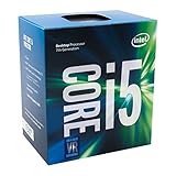
The Core i5 is a CPU series manufactured by Intel aimed at mid-range computers. In this tutorial, we will present a series of quick reference tables for you to compare the main differences between all models released to date. By the way, the correct name of this line of processors is “Core i5,” not “Intel i5.” Currently, there are four different generations of Core i5 processors available. In the table below, we describe the main differences between these generations.
† Except for the model 2390T, which has two cores, supports the Hyper-Threading technology, and has 3 MiB of cache L3. ‡ The 2550K model and models ending with a “P” don’t have integrated video. * Except for the 4570T model, which has two cores and supports the Hyper-Threading technology. Let’s now take a detailed look at all Core i5 models launched so far.
In the table below, we listed all Core i5 6xx and Core i5 7xx CPU models. These are desktop models based on the Nehalem microarchitecture and are also called first-generation Core i5 processors. These models use the socket LGA1156. The integrated memory controller supports dual-channel architecture as well as 1,066 MHz and 1,333 MHz DDR3 memories. They also have an integrated PCI Express 2.0 controller supporting one x16 datapath or two x8 datapaths. Communication with the motherboard chipset is achieved through a DMI bus (1 GB/s per direction, listed as 2.5 GT/s by Intel). All 6xx models have an integrated DirectX 10 video controller with 12 execution units running at 733 MHz or 900 MHz, using an engine that is known as “Intel HD Graphics,” a feature not present on the 7xx models. Models with integrated video support two video monitors. The 7xx models are quad-core CPUs without the Hyper-Threading technology, while the 6xx models are dual-core CPUs using the Hyper-Threading technology. This means that the operating system will recognize all these CPUs as having four cores. However, while on the 7xx models these cores are all “real,” on the 6xx models two of these cores are “real” and the other two are simulated.
sSpec
Model
Clock
Turbo Boost
SLBRP
760
2.80 GHz
3.46 GHz
SLBLH
750S
2.40 GHz
3.20 GHz
SLBLC
750
2.66 GHz
3.20 GHz
SLBTM
680
3.60 GHz
3.86 GHz
SLBLT
670
3.56 GHz
3.73 GHz
SLBTB
661
3.33 GHz
3.60 GHz
SLBNE
661
3.33 GHz
3.60 GHz
SLBTK
660
3.33 GHz
3.60 GHz
SLBLV
660
3.33 GHz
3.60 GHz
SLBXL
655K
3.20 GHz
3.46 GHz
SLBTJ
650
3.20 GHz
3.46 GHz
SLBLK
650
3.20 GHz
3.46 GHz
sSpec
Cores
HT
Video
SLBRP
4
No
No
SLBLH
4
No
No
SLBLC
4
No
No
SLBTM
2
Yes
HD Graphics
SLBLT
2
Yes
HD Graphics
SLBTB
2
Yes
HD Graphics
SLBNE
2
Yes
HD Graphics
SLBTK
2
Yes
HD Graphics
SLBLV
2
Yes
HD Graphics
SLBXL
2
Yes
HD Graphics
SLBTJ
2
Yes
HD Graphics
SLBLK
2
Yes
HD Graphics
sSpec
Model
Video Clock
L3 Cache
SLBRP
760
No
8 MiB
SLBLH
750S
No
8 MiB
SLBLC
750
No
8 MiB
SLBTM
680
733 MHz
4 MiB
SLBLT
670
733 MHz
4 MiB
SLBTB
661
900 MHz
4 MiB
SLBNE
661
900 MHz
4 MiB
SLBTK
660
733 MHz
4 MiB
SLBLV
660
733 MHz
4 MiB
SLBXL
655K
733 MHz
4 MiB
SLBTJ
650
733 MHz
4 MiB
SLBLK
650
733 MHz
4 MiB
sSpec
TDP (W)
Max. Temp. (°C)*
Voltage (V)
SLBRP
95
72.7
0.65 – 1.4
SLBLH
82
76.7
0.65 – 1.4
SLBLC
95
72.7
0.65 – 1.4
SLBTM
73
72.6
0.65 – 1.4
SLBLT
73
72.6
0.65 – 1.4
SLBTB
87
69.8
0.65 – 1.4
SLBNE
87
69.8
0.65 – 1.4
SLBTK
73
72.6
0.65 – 1.4
SLBLV
73
72.6
0.65 – 1.4
SLBXL
73
72.6
0.65 – 1.4
SLBTJ
73
72.6
0.65 – 1.4
SLBLK
73
72.6
0.65 – 1.4
TDP stands for Thermal Design Power and indicates the CPU maximum thermal dissipation, i.e., the CPU cooler must be able to dissipate at least this amount of heat. * The temperatures listed above are Tcase, which is the maximum external temperature of the CPU. On some other models, the manufacturer lists Tjunction, which is the maximum internal temperature of the CPU. The two are not comparable.
The first-generation Core i5 targeted to laptops, named 4xx and 5xx, uses the Nehalem microarchitecture. They can use two different pinouts, BGA1288 or socket G1, and have an integrated dual-channel DDR3 memory controller supporting 800 MHz and 1,066 MHz DDR3 memories. (“UM” models support only DDR3-800 memories.) They have an integrated PCI Express 2.0 controller supporting one x16 connection and an integrated DirectX 10 video controller running at 500 MHz with a 766 MHz “boost” clock (166 MHz with a 500 MHz “boost” clock in “UM” models). Communication with the motherboard chipset is achieved through a DMI bus (1 GB/s per direction, which is listed as 2.5 GT/s by Intel). The models listed below support two video monitors. All Core i5 mobile CPUs are dual-core processors supporting Hyper-Threading (HT) technology, which simulates two logical processing cores in each physical core. Therefore, they are recognized by the operating system as four-core CPUs.
sSpec
Model
Clock
Turbo Boost
SLC28
580M
2.66 GHz
3.33 GHz
SLC29
580M
2.66 GHz
3.33 GHz
SLBSN
560UM
1.33 GHz
2.13 GHz
SLBTS
560M
2.66 GHz
3.20 GHz
SLBTT
560M
2.66 GHz
3.20 GHz
SLBUJ
540UM
1.20 GHz
2.00 GHz
SLBTV
540M
2.53 GHz
3.06 GHz
SLBPF
540M
2.53 GHz
3.06 GHz
SLBPG
540M
2.53 GHz
3.06 GHz
SLBU3
520M
2.40 GHz
2.93 GHz
SLBNA
520M
2.40 GHz
2.93 GHz
SLBNB
520M
2.40 GHz
2.93 GHz
SLBQP
520UM
1.06 GHz
1.86 GHz
SLC27
480M
2.66 GHz
2.93 GHz
SLC26
480M
2.66 GHz
2.93 GHz
SLBXP
470UM
1.33 GHz
1.86 GHz
SLBZW
460M
2.53 GHz
2.80 GHz
SLC22
460M
2.53 GHz
2.80 GHz
SLBTZ
450M
2.40 GHz
2.66 GHz
SLBPM
430M
2.26 GHz
2.53 GHz
SLBPN
430M
2.26 GHz
2.53 GHz
SLBVS
430UM
1.20 GHz
1.73 GHz
sSpec
Cores
HT
Video
SLC28
2
Yes
HD Graphics
SLC29
2
Yes
HD Graphics
SLBSN
2
Yes
HD Graphics
SLBTS
2
Yes
HD Graphics
SLBTT
2
Yes
HD Graphics
SLBUJ
2
Yes
HD Graphics
SLBTV
2
Yes
HD Graphics
SLBPF
2
Yes
HD Graphics
SLBPG
2
Yes
HD Graphics
SLBU3
2
Yes
HD Graphics
SLBNA
2
Yes
HD Graphics
SLBNB
2
Yes
HD Graphics
SLBQP
2
Yes
HD Graphics
SLC27
2
Yes
HD Graphics
SLC26
2
Yes
HD Graphics
SLBXP
2
Yes
HD Graphics
SLBZW
2
Yes
HD Graphics
SLC22
2
Yes
HD Graphics
SLBTZ
2
Yes
HD Graphics
SLBPM
2
Yes
HD Graphics
SLBPN
2
Yes
HD Graphics
SLBVS
2
Yes
HD Graphics
sSpec
Model
Video Clock
Video Boost
Tech.
SLC28
580M
500 MHz
766 MHz
32 nm
SLC29
580M
500 MHz
766 MHz
32 nm
SLBSN
560UM
166 MHz
500 MHz
32 nm
SLBTS
560M
500 MHz
766 MHz
32 nm
SLBTT
560M
500 MHz
766 MHz
32 nm
SLBUJ
540UM
166 MHz
500 MHz
32 nm
SLBTV
540M
500 MHz
766 MHz
32 nm
SLBPF
540M
500 MHz
766 MHz
32 nm
SLBPG
540M
500 MHz
766 MHz
32 nm
SLBU3
520M
500 MHz
766 MHz
32 nm
SLBNA
520M
500 MHz
766 MHz
32 nm
SLBNB
520M
500 MHz
766 MHz
32 nm
SLBQP
520UM
166 MHz
500 MHz
32 nm
SLC27
480M
500 MHz
766 MHz
32 nm
SLC26
480M
500 MHz
766 MHz
32 nm
SLBXP
470UM
166 MHz
500 MHz
32 nm
SLBZW
460M
500 MHz
766 MHz
32 nm
SLC22
460M
500 MHz
766 MHz
32 nm
SLBTZ
450M
500 MHz
766 MHz
32 nm
SLBPM
430M
500 MHz
766 MHz
32 nm
SLBPN
430M
500 MHz
766 MHz
32 nm
SLBVS
430UM
166 MHz
500 MHz
32 nm
sSpec
L3 Cache
TDP (W)
Max. Temp. (°C)*
Package
SLC28
3 MiB
35
105
G1
SLC29
3 MiB
35
105
BGA1288
SLBSN
3 MiB
18
105
BGA1288
SLBTS
3 MiB
35
105
G1
SLBTT
3 MiB
35
105
BGA1288
SLBUJ
3 MiB
18
105
BGA1288
SLBTV
3 MiB
35
105
G1
SLBPF
3 MiB
35
105
BGA1288
SLBPG
3 MiB
35
105
G1
SLBU3
3 MiB
35
105
G1
SLBNA
3 MiB
35
105
BGA1288
SLBNB
3 MiB
35
105
G1
SLBQP
3 MiB
18
105
BGA1288
SLC27
3 MiB
35
105
G1
SLC26
3 MiB
35
105
BGA1288
SLBXP
3 MiB
18
105
BGA1288
SLBZW
3 MiB
35
105
G1
SLC22
3 MiB
35
105
BGA1288
SLBTZ
3 MiB
35
105
G1
SLBPM
3 MiB
35
105
BGA1288
SLBPN
3 MiB
35
105
G1
SLBVS
3 MiB
18
105
BGA1288
TDP stands for Thermal Design Power and indicates the CPU maximum thermal dissipation, i.e., the CPU cooler must be able to dissipate at least this amount of heat. * The temperatures listed above are Tjunction, which is the maximum internal temperature of the CPU. On some other models, the manufacturer lists Tcase, which is the maximum external temperature of the CPU. The two are not comparable.
In the table below, we listed all Core i5-2xxx desktop CPU models, which are based on the Sandy Bridge microarchitecture. They are also called second-generation Core i5 processors and use the socket LGA1155. The integrated memory controller supports dual-channel architecture as well as 1,066 MHz and 1,333 MHz DDR3 memories. They also have an integrated PCI Express 2.0 controller supporting one x16 connection, two x8 connections, one x8 connection or two x4 connections. Communication with the motherboard chipset is achieved through a DMI bus (2 GB/s each direction, listed as 5 GT/s by Intel). All models (except the 2550K and the “P” models) have an integrated DirectX 10.1 video controller running at 650 MHz with a 1.25 GHz “boost” clock or 850 MHz with a 1.1 GHz “boost” clock, with six (HD 2000) or 12 (HD 3000) processing cores. Models with integrated video support two displays. Second-generation Core i5 desktop CPUs with four cores don’t support the Hyper-Threading technology. This means that the operating system will recognize all these CPUs as having four cores. However, while on quad-core models these cores are all “real,” on the dual-core model two of these cores are “real” and the other two are simulated.
sSpec
Model
Clock
Turbo Boost
SR0QH
2550K
3.4 GHz
3.8 GHz
SR00A
2500T
2.3 GHz
3.3 GHz
SR009
2500S
2.7 GHz
3.7 GHz
SR008
2500K
3.3 GHz
3.7 GHz
SR00T
2500
3.3 GHz
3.7 GHz
SR0G1
2450P
3.2 GHz
3.5 GHz
SR0BB
2405S
2.5 GHz
3.3 GHz
SR00S
2400S
2.5 GHz
3.3 GHz
SR00Q
2400
3.1 GHz
3.4 GHz
SR065
2390T
2.7 GHz
3.5 GHz
SR0G2
2380P
3.1 GHz
3.4 GHz
SR02L
2320
3.0 GHz
3.3 GHz
SR02K
2310
2.9 GHz
3.2 GHz
SR00D
2300
2.8 GHz
3.1 GHz
sSpec
Cores
HT
Video
SR0QH
4
No
No
SR00A
4
No
HD 2000
SR009
4
No
HD 2000
SR008
4
No
HD 3000
SR00T
4
No
HD 2000
SR0G1
4
No
No
SR0BB
4
No
HD 3000
SR00S
4
No
HD 2000
SR00Q
4
No
HD 2000
SR065
2
Yes
HD 2000
SR0G2
4
No
No
SR02L
4
No
HD 2000
SR02K
4
No
HD 2000
SR00D
4
No
HD 2000
sSpec
Model
Video Clock
Video Boost
L3 Cache
SR0QH
2550K
No
No
6 MiB
SR00A
2500T
650 MHz
1.25 GHz
6 MiB
SR009
2500S
850 MHz
1.1 GHz
6 MiB
SR008
2500K
850 MHz
1.1 GHz
6 MiB
SR00T
2500
850 MHz
1.1 GHz
6 MiB
SR0G1
2450P
No
No
6 MiB
SR0BB
2405S
850 MHz
1.1 GHz
6 MiB
SR00S
2400S
850 MHz
1.1 GHz
6 MiB
SR00Q
2400
850 MHz
1.1 GHz
6 MiB
SR065
2390T
650 MHz
1.25 GHz
3 MiB
SR0G2
2380P
No
No
6 MiB
SR02L
2320
850 MHz
1.1 GHz
6 MiB
SR02K
2310
850 MHz
1.1 GHz
6 MiB
SR00D
2300
850 MHz
1.1 GHz
6 MiB
sSpec
Tech.
TDP (W)
Max. Temp. (°C)*
Voltage (V)
SR0QH
32 nm
95
72.6
NA
SR00A
32 nm
45
69.8
NA
SR009
32 nm
65
69.1
NA
SR008
32 nm
95
72.6
NA
SR00T
32 nm
95
72.6
NA
SR0G1
32 nm
95
72.6
NA
SR0BB
32 nm
65
69.1
NA
SR00S
32 nm
65
69.1
NA
SR00Q
32 nm
95
72.6
NA
SR065
32 nm
35
65.0
NA
SR0G2
32 nm
95
72.6
NA
SR02L
32 nm
95
72.6
NA
SR02K
32 nm
95
72.6
NA
SR00D
32 nm
95
72.6
NA
TDP stands for Thermal Design Power and indicates the CPU maximum thermal dissipation, i.e., the CPU cooler must be able to dissipate at least this amount of heat. * The temperatures listed above are Tcase, which is the maximum external temperature of the CPU. On some other models, the manufacturer lists Tjunction, which is the maximum internal temperature of the CPU. The two are not comparable.
Last update on 2026-09-16 at 05:35 / Affiliate links / Images from Amazon Product Advertising API
A round-up review comparing the performance of Core 2 Duo E8400, Core 2 Quad Q6600, Phenom X3 8750 and Phenom X4 9550. Which one is the fastest USD 200 CPU? Check it out!
Everything you need to know about relabeled chipsets used on PCChips motherboards, like TX Pro, TX Pro II, VX Pro, VX Pro II, HX Pro, BX Pro, VIA GRA, Xcell 2000, etc.