A8-5600K vs. Pentium G2120 CPU Review
Introduction
Contents
This month AMD released its second-generation of CPUs with integrated video, dubbed “Trinity.” The A8-5600K is a top mid-range model that runs at 3.6 GHz and costs USD 110, competing directly with the Pentium G2120 (3.1 GHz, USD 100) and the Core i3-2100 (3.1 GHz, USD 120).
It is interesting to see AMD starting to use the same letter as Intel to indicate its CPUs with an unlocked clock multiplier, “K.”
This new generation of AMD APUs, dubbed “Trinity,” uses a new CPU socket, called FM2, which is incompatible with the FM1 socket used by the previous generation of APUs (codenamed “llano”). They are physically different, so it is not possible to install an FM1 CPU into an FM2 socket or an FM2 CPU into an FM1 socket. The Pentium and Core i3 CPUs included in our review use the LGA1155 socket.
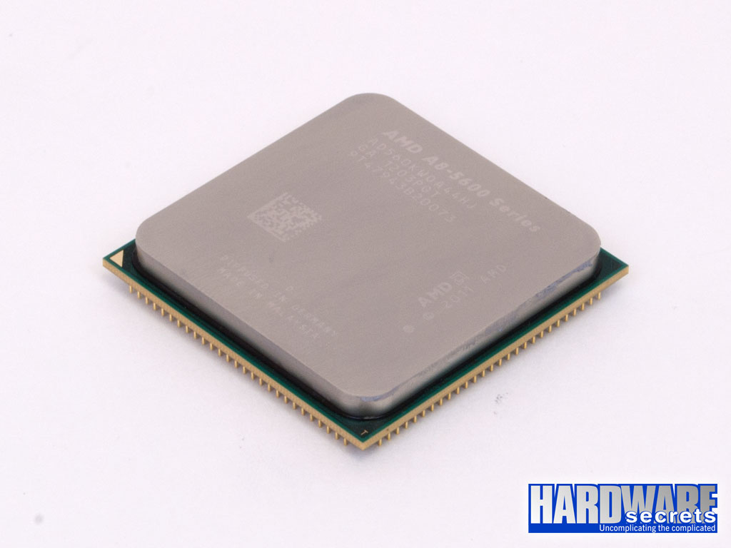 Figure 1: The AMD A8-5600K processor
In the tables below, we compare the main features of the CPUs included in our review. The second-generation APUs (“Trinity”) finally brings support for the SSE4 instruction set (both SSE4.1 and SSE4.2). It also supports the AVX instruction set. More importantly, it has a “turbo clock” technology, which was not available on the previous generation and is not available on Intel’s Pentium and Core i3 processor lines.
The AMD CPUs included in our review are quad-core models, while the Intel CPUs included are dual-core models. However, the Core i3 processors included support the Hyper-Threading (HT) technology, which simulates one additional core per CPU physical core. The operating system “sees” these CPUs as having four cores. This technology is not available on the Pentium CPU, which is one of the main differences between the Core i3 and the current Pentium processors.
It is important to understand that with the second-generation APUs from AMD, each pair of CPU cores share the same front-end engine (i.e., the fetch unit, the L1 instruction cache, and the instruction decoders). So, each pair of CPU cores is part of the same “module,” and the A8-5600K and the A10-5800K are comprised of two of these modules. This concept was introduced with the AMD “Bulldozer” architecture, used on AMD’s FX processor line, and adopted on the “Piledriver” architecture used by the second-generation APUs. With the other CPUs included in our review, each core is a complete CPU, each with its own front-end engine.
| CPU | Cores | HT | SSE4 | AVX | IGP | Clock | Turbo Clock | Base Clock | Codename | Tech. | TDP | Socket | Price |
| A8-3850 | 4 | No | No | No | Yes | 2.9 GHz | No | 100 MHz | Llano | 32 nm | 100 W | FM1 | USD 95 |
| A8-3870K | 4 | No | No | No | Yes | 3.0 GHz | No | 100 MHz | Llano | 32 nm | 100 W | FM1 | USD 105 |
| A8-5600K | 4 | No | Yes | Yes | Yes | 3.6 GHz | 3.9 GHz | 100 MHz | Trinity | 32 nm | 100 W | FM2 | USD 110 |
| A10-5800K | 4 | No | Yes | Yes | Yes | 3.8 GHz | 4.2 GHz | 100 MHz | Trinity | 32 nm | 100 W | FM2 | USD 130 |
| Pentium G2120 | 2 | No | Yes | No | Yes | 3.1 GHz | No | 100 MHz | Ivy Bridge | 22 nm | 55 W | LGA1155 | USD 100 |
| Core i3-2100 | 2 | Yes | Yes | Yes | Yes | 3.1 GHz | No | 100 MHz | Sandy Bridge | 32 nm | 65 W | LGA1155 | USD 120 |
| Core i3-2105 | 2 | Yes | Yes | Yes | Yes | 3.1 GHz | No | 100 MHz | Sandy Bridge | 32 nm | 65 W | LGA1155 | USD 135 |
| Core i3-3220 | 2 | Yes | Yes | Yes | Yes | 3.3 GHz | No | 100 MHz | Ivy Bridge | 22 nm | 55 W | LGA1155 | USD 130 |
Prices were researched at Newegg.com on the day we published this review. TDP stands for Thermal Design Power and states the maximum amount of heat the CPU can dissipate. The CPU cooler must be capable of dissipating at least this amount of heat.
Below you can see the memory configuration for each CPU.
| CPU | L1 Cache (I + D) | L2 Cache | L3 Cache | Memory Support | Memory Channels |
| A8-3850 | 64 KB + 64 KB per core | 1 MB per core | No | Up to DDR3-1866 | Two |
| A8-3870K | 64 KB + 64 KB per core | 1 MB per core | No | Up to DDR3-1866 | Two |
| A8-5600K | 64 kB per module + 16 kB per core | 2 MB x 2 | No | Up to DDR3-1866 | Two |
| A10-5800K | 64 kB per module + 16 kB per core | 2 MB x 2 | No | Up to DDR3-1866 | Two |
| Pentium G2120 | 32 KB + 32 KB per core | 256 kB per core | 3 MB total | Up to DDR3-1600 | Two |
| Core i3-2100 | 32 KB + 32 KB per core | 256 kB per core | 3 MB total | Up to DDR3-1333 | Two |
| Core i3-2105 | 32 KB + 32 KB per core | 256 kB per core | 3 MB total | Up to DDR3-1333 | Two |
| Core i3-3220 | 32 KB + 32 KB per core | 256 kB per core | 3 MB total | Up to DDR3-1333 | Two |
Below we have a quick comparison of the video engine of the CPUs.
| CPU | Video Engine | DirectX | Clock | Cores |
| A8-3850 | Radeon HD 6550D | 11 | 600 MHz | 400 |
| A8-3870K | Radeon HD 6550D | 11 | 600 MHz | 400 |
| A8-5600K | Radeon HD 7560D | 11 | 760 MHz | 256 |
| A10-5800K | Radeon HD 7660D | 11 | 800 MHz | 384 |
| Pentium G2120 | Intel HD Graphics | 11 | 650 MHz/1.05 GHz | 6 |
| Core i3-2100 | Intel HD 2000 | 10.1 | 850 MHz/1.1 GHz | 6 |
| Core i3-2105 | Intel HD 3000 | 10.1 | 850 MHz/1.1 GHz | 12 |
| Core i3-3220 | Intel HD 2500 | 11 | 650 MHz/1.05 GHz | 6 |